High density plasma process for the formation of silicon dioxide on silicon carbide substrates

a silicon carbide substrate and high density plasma technology, applied in the direction of crystal growth process, coating, chemical apparatus and processes, etc., can solve the problems of affecting the mobility of carriers, and affecting the performance of sic mosfets, etc., to achieve high performance, improve the growth/deposition of sio2 films, and reduce thermal budgets

Active Publication Date: 2005-09-29
SHARP KK
View PDF7 Cites 24 Cited by
  • Summary
  • Abstract
  • Description
  • Claims
  • Application Information

AI Technical Summary

Benefits of technology

[0009] The present invention describes a novel growth / deposition method for the fabrication of SiO2 thin films by high-density plasma-based processes, employing an inductively coupled plasma source. The high-density plasma processes generate high electron / ion concentrations, with suitable electron temperatures, to enhance the growth / deposition of SiO2 film on SiC. The high-density plasma process is characterized by high electron / ion concentration, low plasma potential, and independent control of plasma energy and density. The high-density plasma growth / deposition process is effective in controlling the bulk and interfacial properties of the SiO2 thin film, which are critical for the fabrication of high performance and reliable electronic devices. The high electron / ion energy, low plasma potential, and high electron temperature of the high-density ICP plasma process make it possible to fabricate SiO2 thin films at significantly lower thermal budgets, as compared to the conventional thermal, and plasma-based physical and chemical techniques.

Problems solved by technology

However, Si-based devices, including MOSFETs, fail under extreme operating conditions, such as high temperature, high power, and high radiation.
However, SiC MOSFET performance is hampered by a high density of interface states.
As a result, carrier mobility is significantly reduced and the current (power) handling capability of these devices is much lower than would otherwise be expected.
The thermal oxidation of SiC is typically carried out at temperatures in the range of 1000-1300° C. This high-temperature thermal oxidation process can be harmful to some conventionally used IC materials such as glass or plastic.
However, oxidation at lower temperatures conventionally requires excessively long oxidation times.

Method used


Image

  • High density plasma process for the formation of silicon dioxide on silicon carbide substrates
  • High density plasma process for the formation of silicon dioxide on silicon carbide substrates
  • High density plasma process for the formation of silicon dioxide on silicon carbide substrates

Examples


Embodiment Construction

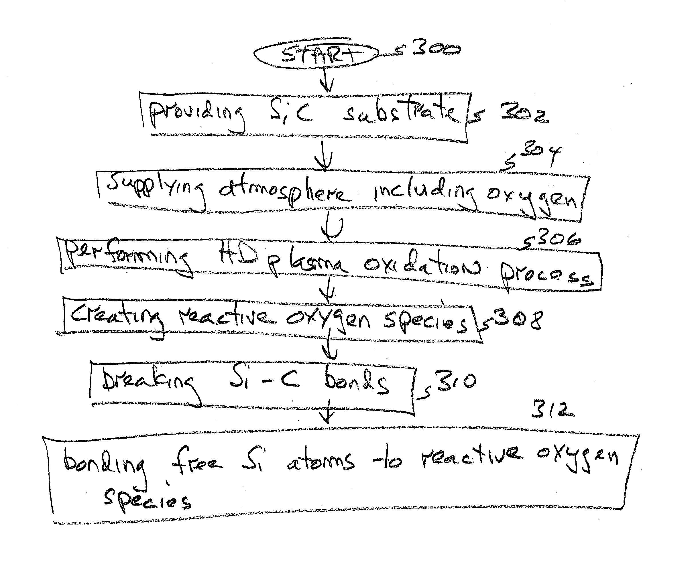
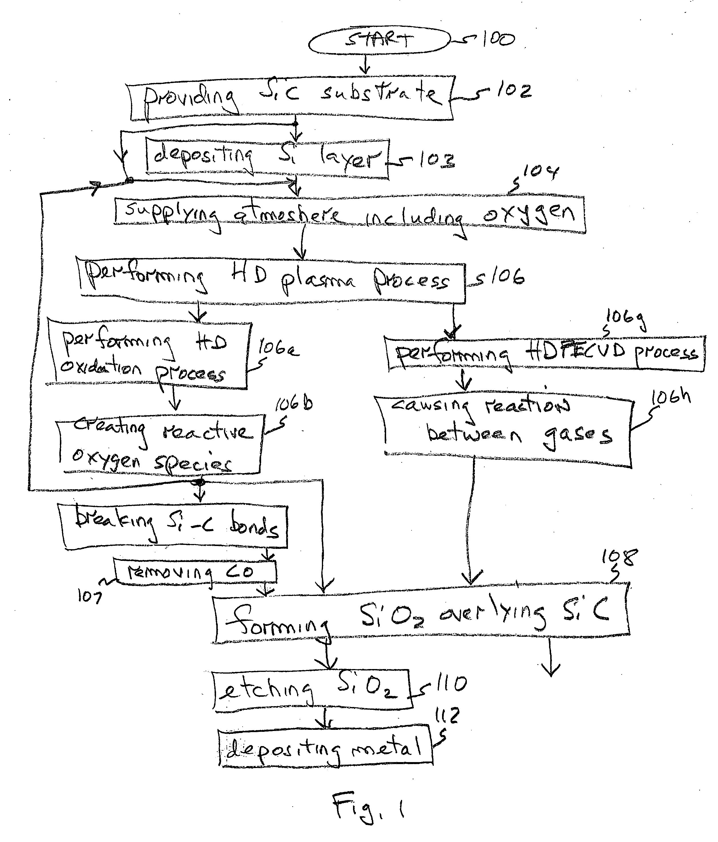
[0027]FIG. 1 is a flowchart generally illustrating the present invention method for forming silicon dioxide (SiO2) on a silicon carbide (SiC) substrate. Although the method (and the methods described below) is depicted as a sequence of numbered steps for clarity, no order should be inferred from the numbering unless explicitly stated. It should be understood that some of these steps may be skipped, performed in parallel, or performed without the requirement of maintaining a strict order of sequence. The method starts at Step 100.

[0028] Step 102 provides a SiC substrate. Step 104 supplies an atmosphere including oxygen. Step 106 performs a high-density (HD) plasma-based process. Step 108 forms a SiO2 layer overlying the SiC substrate. Preferably, performing an HD plasma-based process in Step 106 includes connecting a top electrode to an inductively coupled HD plasma source.

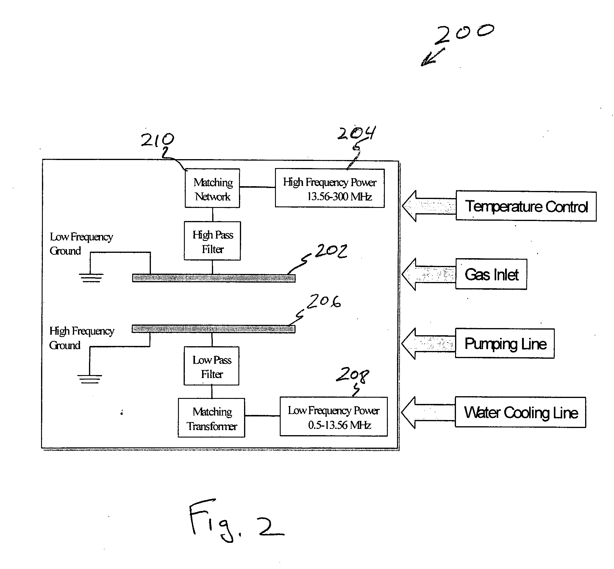
[0029]FIG. 2 is a schematic block diagram of an inductively coupled high-density plasma source. Although an in...


PUM

PropertyMeasurementUnit
frequencyaaaaaaaaaa
frequencyaaaaaaaaaa
pressureaaaaaaaaaa

Abstract

Methods are provided for forming silicon dioxide (SiO2) on a silicon carbide (SiC) substrate. The method comprises: providing a SiC substrate; supplying an atmosphere including oxygen; performing a high-density (HD) plasma-based process; and, forming a SiO2 layer overlying the SiC substrate. Typically, performing the HD plasma-based process includes connecting a top electrode to an inductively coupled HD plasma source. In one aspect, SiO2 is grown on the SiC substrate. Then, an HD plasma oxidation process is performed that creates a reactive oxygen species and breaks the Si—C bonds in the SiC substrate, to form free Si and C atoms in the SiC substrate. The free Si atoms in the SiC substrate are bonded to the HD plasma-generated reactive oxygen species, and the SiO2 layer is grown.

Description

RELATED APPLICATIONS [0001] This application is a continuation-in-part of a pending patent application entitled, METHODS FOR FABRICATING OXIDE THIN FILMS, invented by Joshi et al., Serial No. ______, filed ______, Attorney Docket No. SLA787. [0002] This application is a continuation-in-part of a pending patent application entitled, DEPOSITION OXIDE WITH IMPROVED OXYGEN BONDING, invented by Pooran Joshi, Serial No. ______, filed ______, Attorney Docket No. SLA766.BACKGROUND OF THE INVENTION [0003] 1. Field of the Invention [0004] This invention generally relates to integrated circuit (IC) fabrication and, more particularly, to a system and method for forming silicon dioxide films overlying a silicon carbide substrate, [0005] 2. Description of the Related Art [0006] The silicon-based (silicon substrate) MOSFET is the most commonly manufactured electronic device, worldwide. However, Si-based devices, including MOSFETs, fail under extreme operating conditions, such as high temperature, ...

Claims


Application Information

Patent Timeline
Patent Type & Authority Applications(United States)
IPC IPC(8): B05D5/12C23C16/02C23C16/40H01L29/872C23C16/509C30B1/00H01L21/00H01L21/04H01L21/20H01L21/31H01L21/316H01L21/36H01L21/469H01L29/47
CPCC23C16/0272C23C16/402C23C16/509H01L21/02164H01L21/0223H01L21/31612H01L21/02252H01L21/02274H01L21/045H01L21/049H01L21/02238
Inventor JOSHI, POORAN CHANDRAVOUTSAS, APOSTOLOS T.HARTZELL, JOHN W.
Owner SHARP KK
Why Eureka
Try Eureka