Data transfer method and electronic device

a data transfer and electronic device technology, applied in the field of data transfer methods and electronic devices, can solve the problems of increasing the number of wires and large current consumption, and achieve the effect of reducing the emi

Active Publication Date: 2005-10-06
AU OPTRONICS CORP
View PDF14 Cites 82 Cited by
  • Summary
  • Abstract
  • Description
  • Claims
  • Application Information

AI Technical Summary

Benefits of technology

[0011] As a result of the means described above, the transfer of data between second semiconductor integrated circuits with a large wiring resistance in comparison with a transfer between a first semiconductor integrated circuit and an initial-stage second semiconductor integrated circuit is performed by means of a CMOS signal with a long cycle and large amplitude (driving capacity) by means of a differential signal, whereby a setup / hold margin can be adequately obtained when the data is captured by each semiconductor integrated circuit.
[0012] The present invention makes it possible to reduce the EMI, current consumption and so forth in an interchip transfer of data and a timing signal and to provide an appropriate timing margin for the capture of data.

Problems solved by technology

Although high-speed transfers of clock signals, display data, and so forth are required between the controller and data drivers within a liquid crystal display module, there has been the problem that, in the case of a conventional CMOS interface, the number of wires increases when the parallel transmission system must be adopted in order to prevent EMI (Electromagnetic Interference) noise.
Further, in cases where an RSDS interface is used in the transfer of display data between data drivers, there is the problem that a fixed current must flow in order to transmit the RSDS signal and the current consumption is large.

Method used


Image

  • Data transfer method and electronic device
  • Data transfer method and electronic device
  • Data transfer method and electronic device

Examples


Embodiment Construction

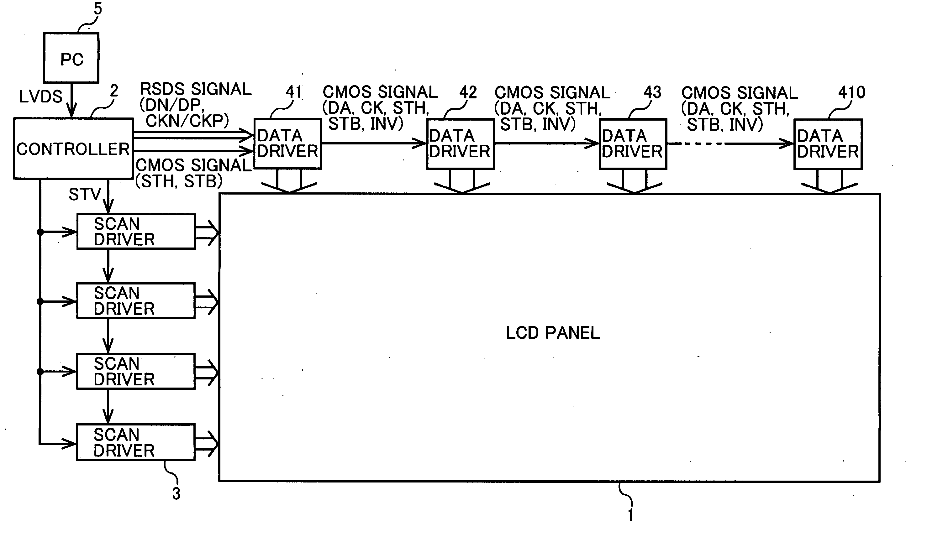
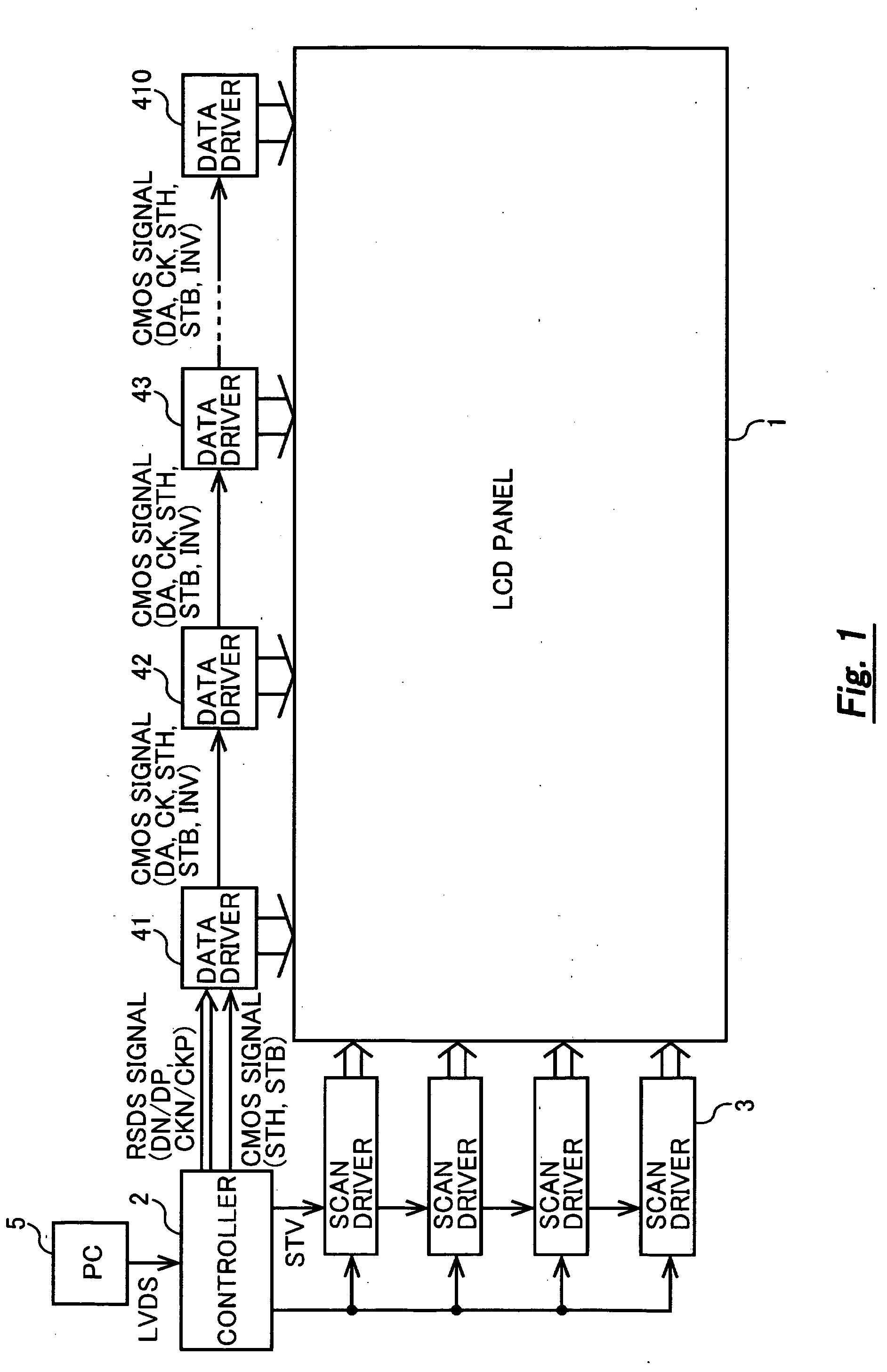
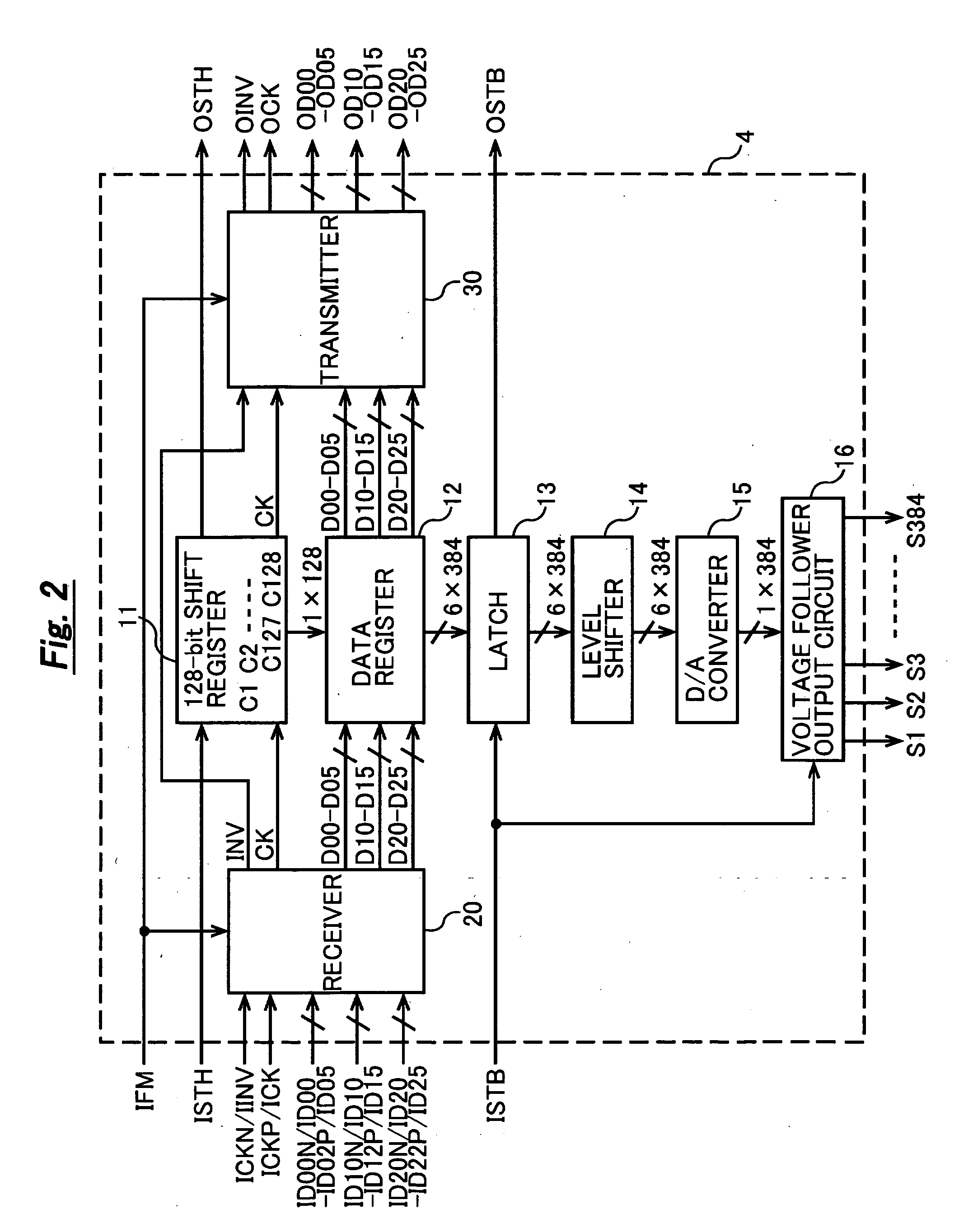
[0027] Where the codes for the display data, timing signal, and so forth used in the following description are concerned, CMOS signals and RSDS signals are defined below for the purposes of clarification.

[0028] (1) Display data DATA: no distinction between CMOS signal, RSDS signal, and so forth

[0029] (2) Display data DA: CMOS signal

[0030] (3) Display data D00 to D05, D10 to D15, D20 to D25: CMOS signal

[0031] (4) Display data DN / DP: RSDS signal

[0032] (5) Display data D00N / D00P to D02N / D02P, D10N / D10P to D12N / D12P, D20N / D20P to D22N / D22P: RSDS signal

[0033] (6) Clock signal CLK: no distinction between CMOS signal, RSDS signal, and so forth

[0034] (7) Clock signal CK: CMOS signal

[0035] (8) Clock signal CKN / CKP: RSDS signal

[0036] (9) Start signal STH, latch signal STB, data inversion signal INV: CMOS signal

[0037] The invention will be now described herein with reference to illustrative embodiments. Those skilled in the art will recognize that many alternative embodiments can be ...


PUM

PropertyMeasurementUnit
clock frequencyaaaaaaaaaa
DAaaaaaaaaaa
DAaaaaaaaaaa

Abstract

The present invention provides a liquid-crystal display device that is able to reduce EMI, current consumption, and so forth in an interchip transfer of display data, a timing signal, and so forth and to provide an appropriate timing margin. In an interchip transfer of display data, a timing signal, and so forth that uses a plurality of data drivers, a certain data driver is used as a data driver. When the data driver is used in a first stage, an internal receiver is made to function as an RSDS receiver by fixing the IFM terminal at the “H” level. The received RSDS signal constitutes a CMOS signal that has been divided into two by the receiver and is output by the transmitter. Here, a data inversion signal is generated and output by the transmitter. When the data driver is used in the second or subsequent stage, the internal receiver is made to function as a CMOS receiver by fixing the IFM terminal at the “L” level. The received CMOS signal is output after being subjected to inversion control by means of the data inversion signal by the receiver and transmitter.

Description

BACKGROUND OF THE INVENTION [0001] 1. Field of the Invention [0002] The present invention relates to a data transfer method and electronic device and, more particularly, to a data transfer method and electronic device whereby data is sequentially transferred to a plurality of cascade-connected semiconductor integrated circuits. [0003] 2. Description of the Related Art [0004] Liquid crystal display devices are used as dot matrix-type display devices in a variety of devices such as personal computers based on the merits of their thin form, light weight, and low power, with active matrix-type color liquid crystal display devices, which are useful in controlling images in particular highly accurately, holding the mainstream. [0005] A liquid crystal display module of a liquid crystal display device comprises a liquid crystal panel (LCD panel), a control circuit (referred to as a ‘controller’ hereinbelow) consisting of a semiconductor integrated circuit device (referred to as an ‘IC’ here...

Claims


Application Information

Patent Timeline
Patent Type & Authority Applications(United States)
IPC IPC(8): G02F1/133G09G3/20G09G3/36
CPCG09G3/20G09G3/3611G09G3/3688G09G2330/06G09G2310/08G09G2330/021G09G2310/027
Inventor FUKUO, MOTOO
Owner AU OPTRONICS CORP
Why Eureka
Try Eureka