

Methods for modifying carbon nanotube structures to enhance coating optical and electronic properties of transparent conductive coatings
a technology of carbon nanotubes and carbon nanotubes, which is applied in the direction of carbon-silicon compound conductors, coatings, chemistry apparatuses and processes, etc., can solve the problems of large capital expenditure and difficulty in scaling up, and achieve the effect of increasing the optical and electrical properties of carbon nanotube-based transparent electrically conductive coatings
- Summary
- Abstract
- Description
- Claims
- Application Information
AI Technical Summary
Benefits of technology
Problems solved by technology
Method used
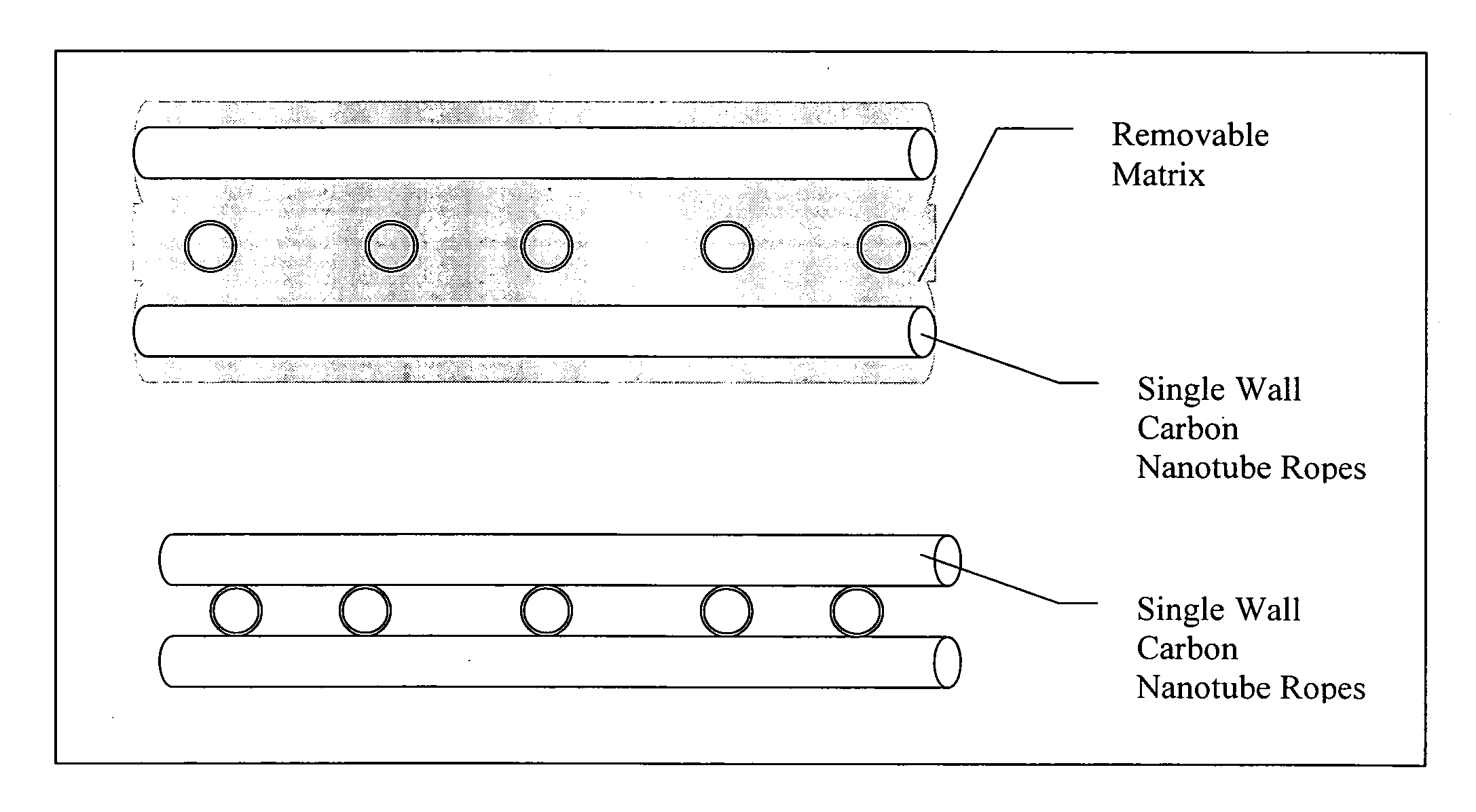
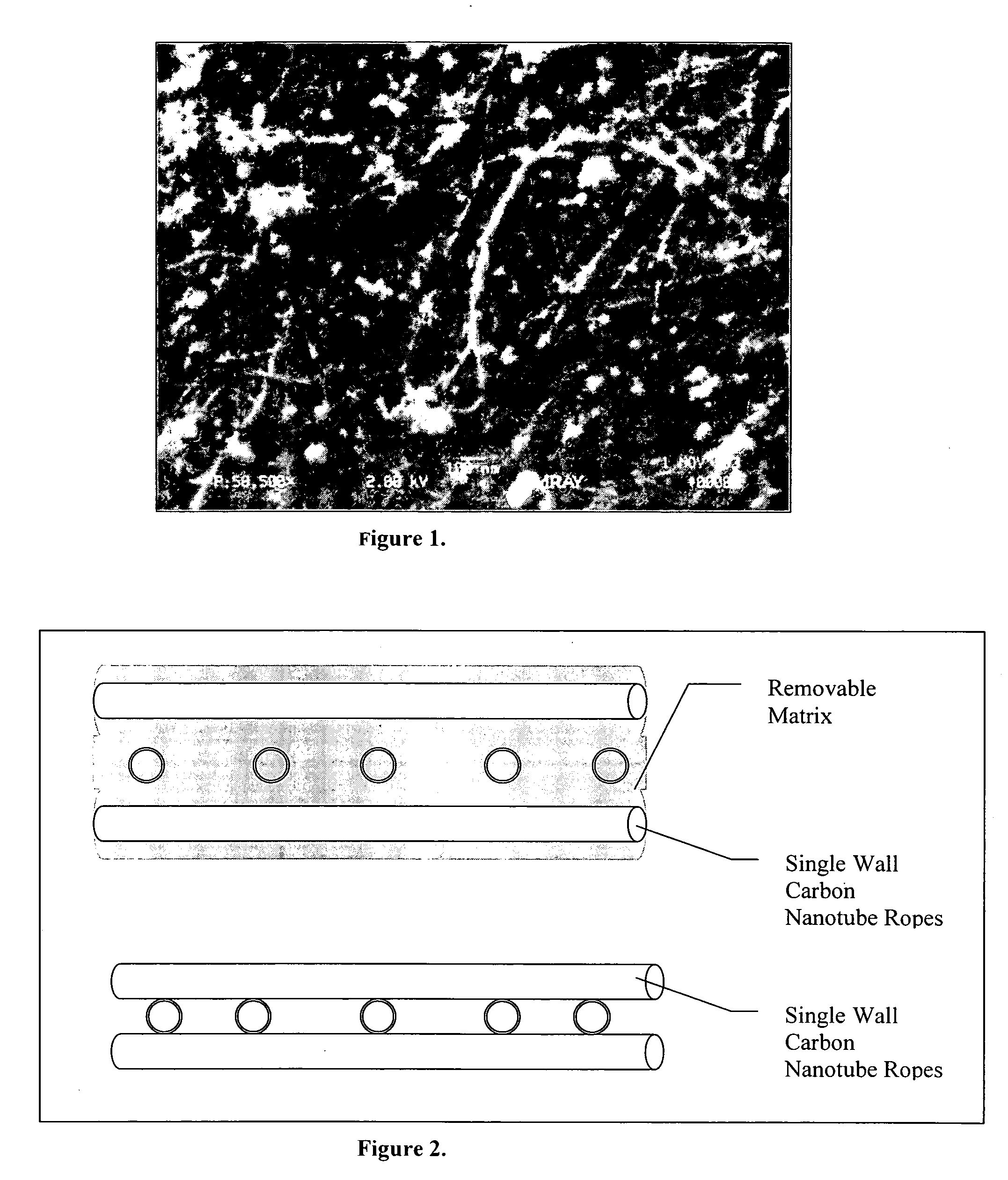
Image

Examples
example 1
Use of Water and Standard Laboratory Branson Ultrasonic Bath to Increase Transparence and Reduce Resistivity in CNT Coated PET Film
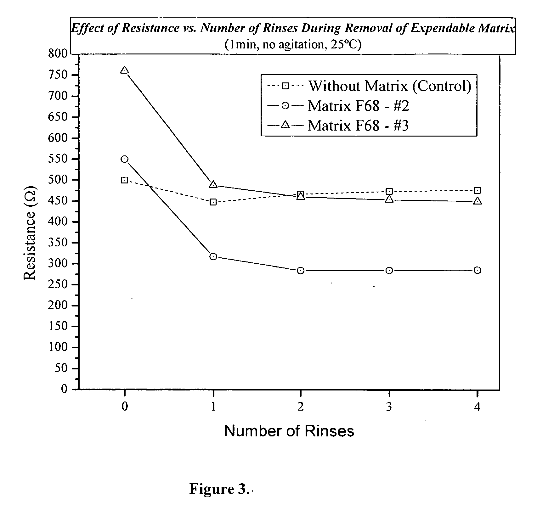
[0027] The experiment started with a 5-mil PET film ST 505 film, having bands of silver paint placed four inches apart to form a square area for testing. The entire PET film was spray coated with Eikos' SWCnT ink (SWCnT suspend in water / alcohol solvent) using an airbrush (i.e. Paasche VLS#3) to a surface resistivity of below 500 Ohms / Square. This sample was then died in air at 100° C. for 10 minutes. The electrical and optical properties were then measured in air. The sample was then placed in a round glass container filled with purified water. The ultrasonic bath was turned on and the container with the film sample was lowered into the bath for the stated seconds. The film was then dried in air for 10-minutes before taking the next resistance reading.
[0028] The SWCnT coated PET sample that did not have a binder improved in both transparency and electr...
example 2
Glass Slides Coated with CNT and Rinsed to Increase Optical Transparency and Reduce Electrical Resistivity
[0029] Four experimental trials applying the methods described above to increase optical and electrical performance of SWCnT coatings.
[0030] In trials #1 and #2, arc produced single walled carbon nanotube soot containing approximately 50-60% carbon nanotubes was purified by refluxing in 3M nitric acid solution for 18 hours at 145±15° C. The mixture was rinsed and centrifuged to produced an ink solution containing >99% single walled carbon nanotubes at a concentration of 0.189 g / L (ink solution “A”).
[0031] The ink formulations sprayed in trials #1 and #2 were performed utilizing an airbrush at 25-30 psi air assist pressure onto a heated (75° C.) 1″×3″ glass slide with silver electrodes spaced 1″ apart. The spacing provides two (2) measurements of sheet resistance and percent transmitted light on each slide. The application of SWCnT was performed until a predetermined amount (s...
PUM
| Property | Measurement | Unit |
|---|---|---|
| Electronic properties | aaaaa | aaaaa |
| Optical properties | aaaaa | aaaaa |
Abstract
Description
Claims
Application Information