

Electrodepositing a metal in integrated circuit applications
- Summary
- Abstract
- Description
- Claims
- Application Information
AI Technical Summary
Benefits of technology
Problems solved by technology
Method used
Image

Examples
Embodiment Construction
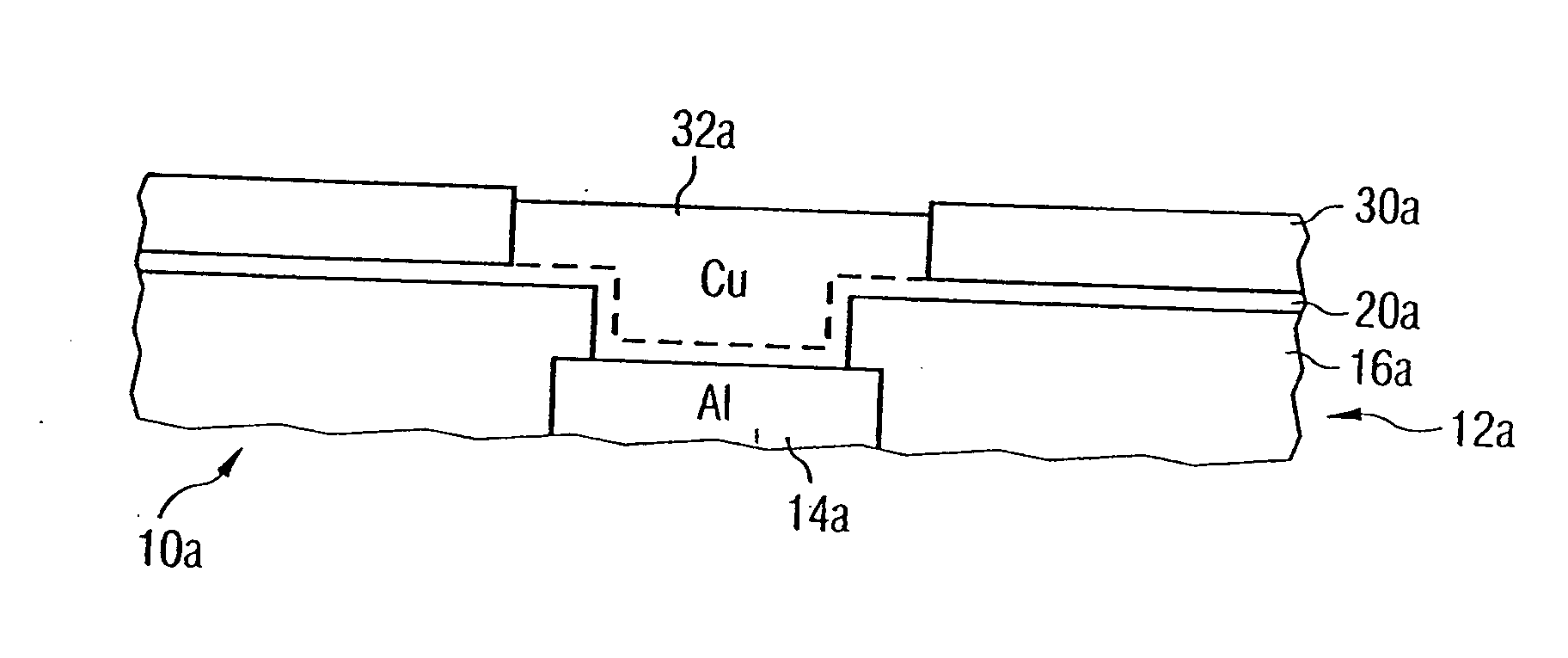
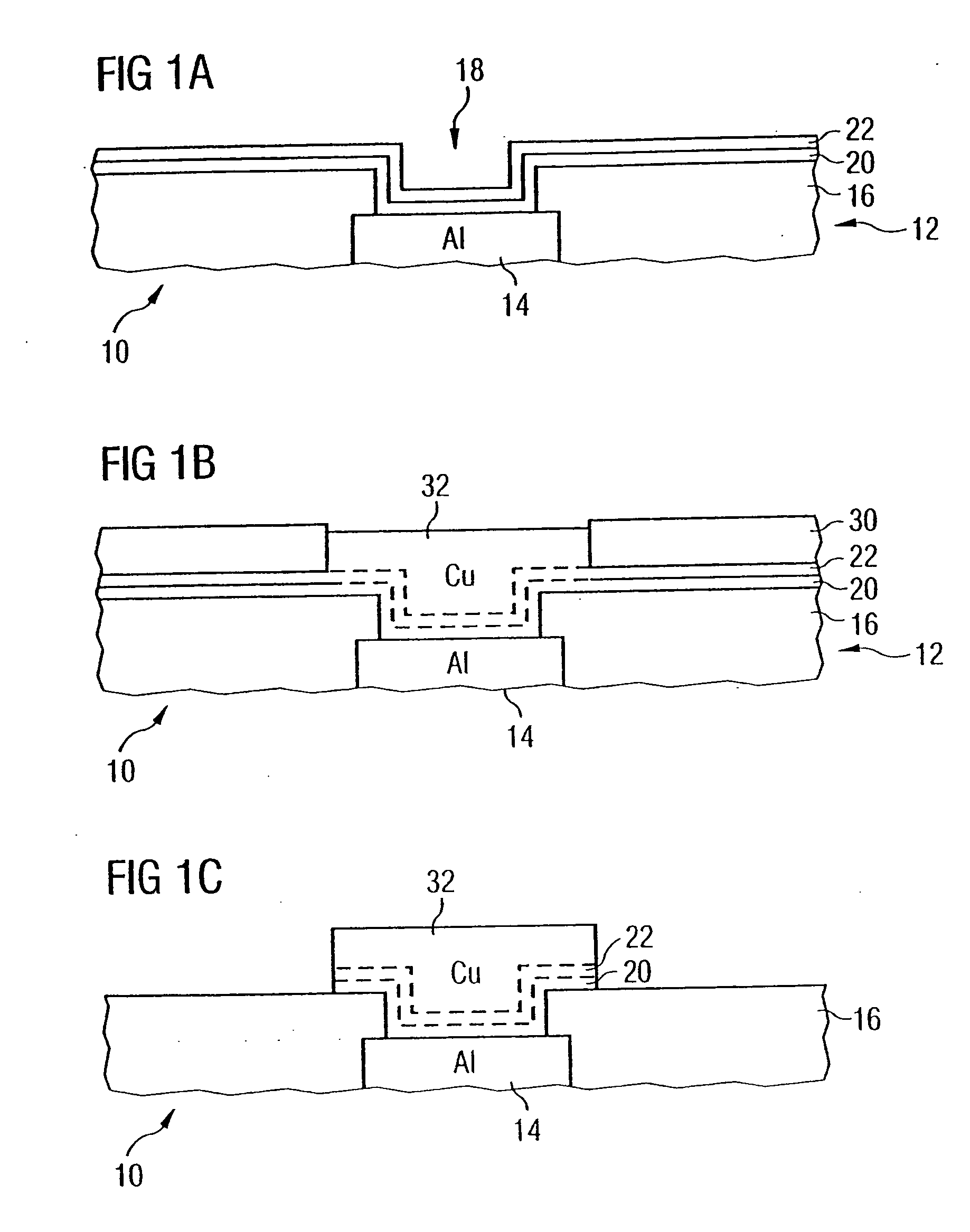
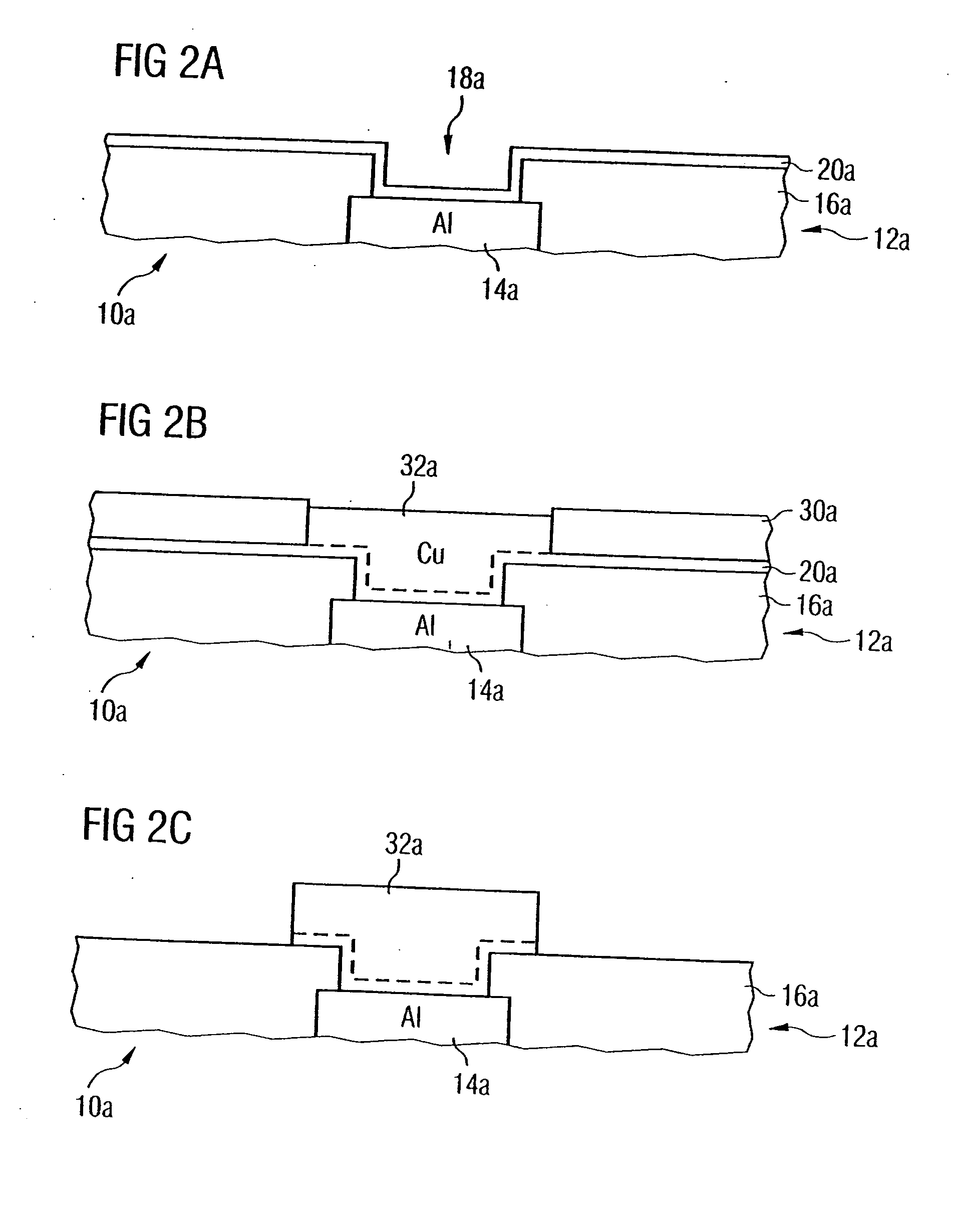
[0013] A method for electrodepositing a metal will now be described more fully with reference to the accompanying drawings. In each of the following figures, components, features and integral parts that correspond to one another each have the same reference number. The drawings of the figures are not true to scale.
[0014] In semiconductor production, in which copper may be used in metallization planes, it is desired to separate a Front End Of Line (FEOL) production and a Back End Of Line (BEOL). FEOL production relates, inter alia, to method steps for fabricating Shallow Trench Isolation (STI), Local Oxidation of Silicon insulations (LOCOS), the fabrication of transistors, including the required implantations. BEOL production relates, inter alia, to the fabrication of metallization and passivation planes. By way of example, if only the last metallization layer is fabricated using a metal whose atoms have a large diffusion coefficient in silicon, then BEOL production is again subdivi...
PUM
| Property | Measurement | Unit |
|---|---|---|
| Temperature | aaaaa | aaaaa |
| Fraction | aaaaa | aaaaa |
| Percent by mass | aaaaa | aaaaa |
Abstract
Description
Claims
Application Information