Plasma processing apparatus

a processing apparatus and plasma technology, applied in the direction of electrical apparatus, plasma technique, electric discharge tubes, etc., can solve the problems of non-uniform circumferential (azimuthal) direction of reaction on the wafer surface, non-uniform circumferential direction of plasma, etc., to facilitate the determination process, enhance plasma processing performance and controllability of the apparatus as a whole, and facilitate the effect of processing

Inactive Publication Date: 2005-10-13
HITACHI HIGH-TECH CORP
View PDF5 Cites 20 Cited by
  • Summary
  • Abstract
  • Description
  • Claims
  • Application Information

AI Technical Summary

Benefits of technology

[0032] According to such configurations, it is possible to dispose a parallel coil having a large number of total turns in a limited space.
[0033] According to the present plasma processing apparatus, complete plasma uniformity across the circumferential direction can be achieved. Therefore, the plasma etch result is uniform in the circumferential direction, and since it is necessary only to consider the uniformity in the radial direction when determining plasma etching process conditions, the determination process is facilitated and prompt. As a result, the plasma processing performance and the controllability of the apparatus as a whole is enhanced, and it becomes possible to provide finer etching process with high throughput, and higher quality film deposition and surface treatment.

Problems solved by technology

It is desirable that the wafer etching is completely uniform across the wafer surface, but in actual, the reaction on the wafer surface is not completely uniform due to the non-uniform distribution of plasma, dissociated species and reaction products within the reaction chamber.
However, in an inductively coupled plasma processing apparatus, non-uniformity in the circumferential (azimuthal) direction occurs due to the configuration of the apparatus.
That is, a coil always has an end connected to the RF power supply and another end connected to ground, and this coil configuration causes plasma non-uniformity in the circumferential direction.
However, according to such arrangement, along with the increase of the number of coils, the power supply to the coils is restricted to be supplied only from the center of the arrangement, by which the limitation regarding the design of the apparatus becomes great.
The increased voltage causes the plasma to have better ignition property and low-density stability, but on the one hand, causes increase of damage caused by ion sputtering of the insulating member disposed between the induction coil and plasma.
On the other hand, design-related problems occur by the increased current, such as heating, the loss caused thereby, and current resistance of the variable capacitor used in the matching network.
The increase in voltage causes problems such as abnormal discharge, undesirable effect to plasma, and voltage resistance of the variable capacitor.
However, the difficulty of adopting a parallel coil is that the space for disposing the induction coil is limited from the viewpoint of apparatus design.

Method used


Image

  • Plasma processing apparatus
  • Plasma processing apparatus
  • Plasma processing apparatus

Examples


first embodiment

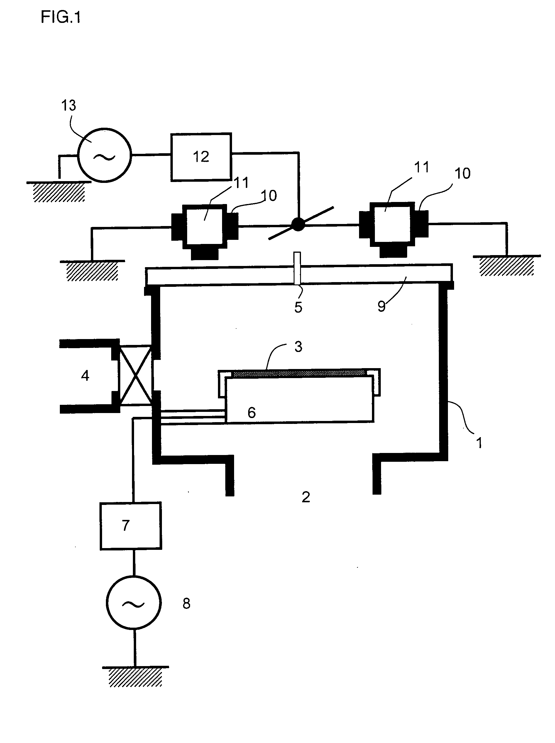
[0049] With reference to FIG. 1, an arrangement corresponding to a plasma processing apparatus according to the present invention will be described. An RF inductively coupled plasma processing apparatus comprises a processing chamber 1 maintained in vacuum, an evacuation means 2 connected to a vacuum pump for example for maintaining the interior of the processing chamber in vacuum, a wafer-transfer system 4 for carrying a semiconductor wafer 3 or object to be processed into and out of the vacuum processing chamber, an inlet 5 for introducing processing gas, an electrode 6 on which the semiconductor wafer 3 is placed (sample stage for mounting the object to be processed), a matching network 7, an RF power supply 8, an insulator 9 functioning as the ceiling of the processing chamber and through which the electric field created by radio frequency is introduced to the processing chamber, an RF induction coil 10 having an arrangement unique to the present invention, an annular insulating...

embodiment 3

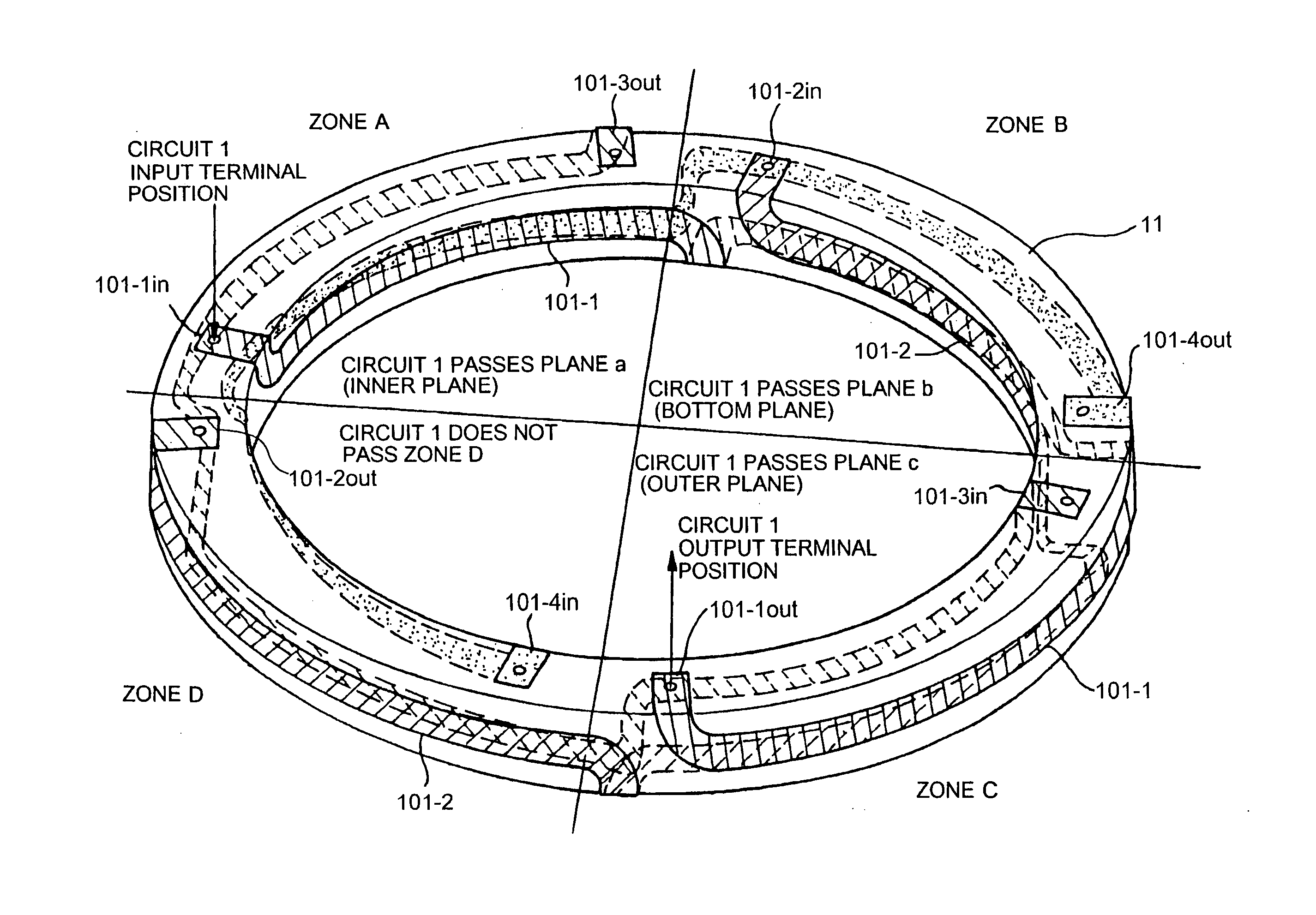
[0059] In this example, four circuits of ¾-turn coil elements are used, totaling in three turns. FIG. 6 is a perspective view showing the actual coil formed in this manner (embodiment 3). Unlike the example shown in FIG. 4 where the coil elements are disposed flatly, the present embodiment utilizes space advantageously and successfully creates a compact induction coil 10. By adopting this induction coil to the plasma processing apparatus illustrated in FIG. 1, it is possible to provide a plasma processing apparatus having advantageous circumferential plasma uniformity.

[0060] In the example of Table 1, each coil element is passed via adjacent planes, from plane a to plane b to plane c, but it is also possible to have the coil pass via plane a to plane c and then to plane b, as shown in Table 2. It may seem irrational to pass the coil from plane a directly to plane c, but since these planes are in confronting relations, the coil can be passed through a bore pierced through the insulat...

embodiment 7

[0064] In order to increase the number of turns, it may be possible to use an insulating ring 11 having a polygonal cross-section with more than four sides. This embodiment 7 will be illustrated with reference to FIG. 10 and table 6. The present embodiment uses an insulating ring 11 with an octagonal cross-section. The surfaces are denoted as planes a through h as illustrated, and through use of seven planes excluding the upper plane, plane h, coil loops are arranged in a manner similar to the embodiment of FIG. 5, wherein the coil element of circuit 1 is first disposed on plane a in zone A and extended via planes b, c, d, e, f and g transiting planes every 90°, and the coil element of circuit 2 is first disposed on plane a in zone B and extended via planes b, c, d, e, f and g transiting planes every 90°, thereby forming loops. A single coil element circuit constitutes 7 / 4 turns, so by disposing four circuits, the induction coil totals in seven turns.

TABLE 6Planes used: 7, 7 / 4-turn ...


PUM

PropertyMeasurementUnit
radio frequencyaaaaaaaaaa
inductanceaaaaaaaaaa

Abstract

The invention provides an inductively coupled plasma apparatus capable of disposing a parallel coil with a large number of total turns in a relatively small space. The present plasma processing apparatus comprises a processing chamber for subjecting an object to plasma processing, an inlet means for introducing a processing gas into the processing chamber, an evacuation means for evacuating an interior of the processing chamber, a sample stage for placing the object, a power supply means for generating plasma, and at least one induction coil connected to the power supply means, wherein the induction coil is formed by connecting a plurality of identical coil elements 101 in a parallel circuit-like arrangement, the induction coil being positioned so that its center corresponds to a center of the object, and wherein input ends 101 in of the coil elements 101 are arranged at equal angular intervals calculated by dividing 360° by the number of coil elements, the coil elements having a three-dimensional structure in a radial direction and a height direction along a surface of an annular ring with an arbitrary cross-sectional shape.

Description

[0001] The present application is based on and claims priority of Japanese patent application No. 2004-117894 filed on Apr. 13, 2004, the entire contents of which are hereby incorporated by reference. FIELD OF THE INVENTION [0002] The present invention relates to a plasma processing apparatus preferably used for etching objects or depositing films in the process of manufacturing semiconductor devices, liquid crystal display substrates or the like. DESCRIPTION OF THE RELATED ART [0003] Along with the miniaturization of semiconductor devices, process conditions (process window) of a plasma process that realizes uniform processing to be carried out across the whole wafer surface have become narrower, so there are increasing demands for plasma processing apparatuses having more complete control of the states of the processes. In order to answer to such demands, it is required a plasma processing apparatus capable of controlling the plasma distribution, the process gas dissociation and t...

Claims


Application Information

Patent Timeline
Patent Type & Authority Applications(United States)
IPC IPC(8): H05H1/46C23F1/00H01J37/32H01L21/205H01L21/3065
CPCH01J37/321
Inventor EDAMURA, MANABUMIYA, GOYOSHIOKA, KEN
Owner HITACHI HIGH-TECH CORP
Why Eureka
Try Eureka