Light-emitting device having pnpn structure and light-emitting device array

Inactive Publication Date: 2005-10-13
FUJIFILM BUSINESS INNOVATION CORP
View PDF2 Cites 21 Cited by
  • Summary
  • Abstract
  • Description
  • Claims
  • Application Information

AI Technical Summary

Benefits of technology

[0015] An object of the present invention is to provide a self-scanning light-emit

Problems solved by technology

A digital circuit has a tendency to decrease its power supply voltage for the requirements of higher speed and lower cons

Method used


Image

  • Light-emitting device having pnpn structure and light-emitting device array
  • Light-emitting device having pnpn structure and light-emitting device array
  • Light-emitting device having pnpn structure and light-emitting device array

Examples


embodiment 1

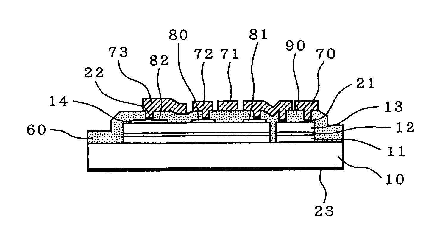
[0052] The present embodiment is directed to a light-emitting element having a schottky contact terminal on a gate layer of a PNPN-structure. A device structure of a light-emitting element formed in a chip is shown in FIG. 3 in which FIG. 3A is a plan view and FIG. 3B is a cross-sectional view taken along X-X line in FIG. 3A. On a first conductivity-type of GaAs substrate 10, there are stacked a first conductivity-type AlGaAs epitaxial layer 11, a second conductivity-type AlGaAs epitaxial layer 12, a first conductivity-type AlGaAs epitaxial layer 13, and a second conductivity-type AlGaAs epitaxial layer 14 in this order to form a PNPN-structure. A light-emitting thyristor is fabricated using this PNPN-structure.

[0053] The light-emitting thyristor comprises an ohmic electrode 21 formed an the first conductivity-type AlGaAs layer 13, an ohmic electrode 22 formed on the second conductivity-type AlGaAs layer 14, and an ohmic electrode (a common electrode) formed on a bottom surface of ...

embodiment 2

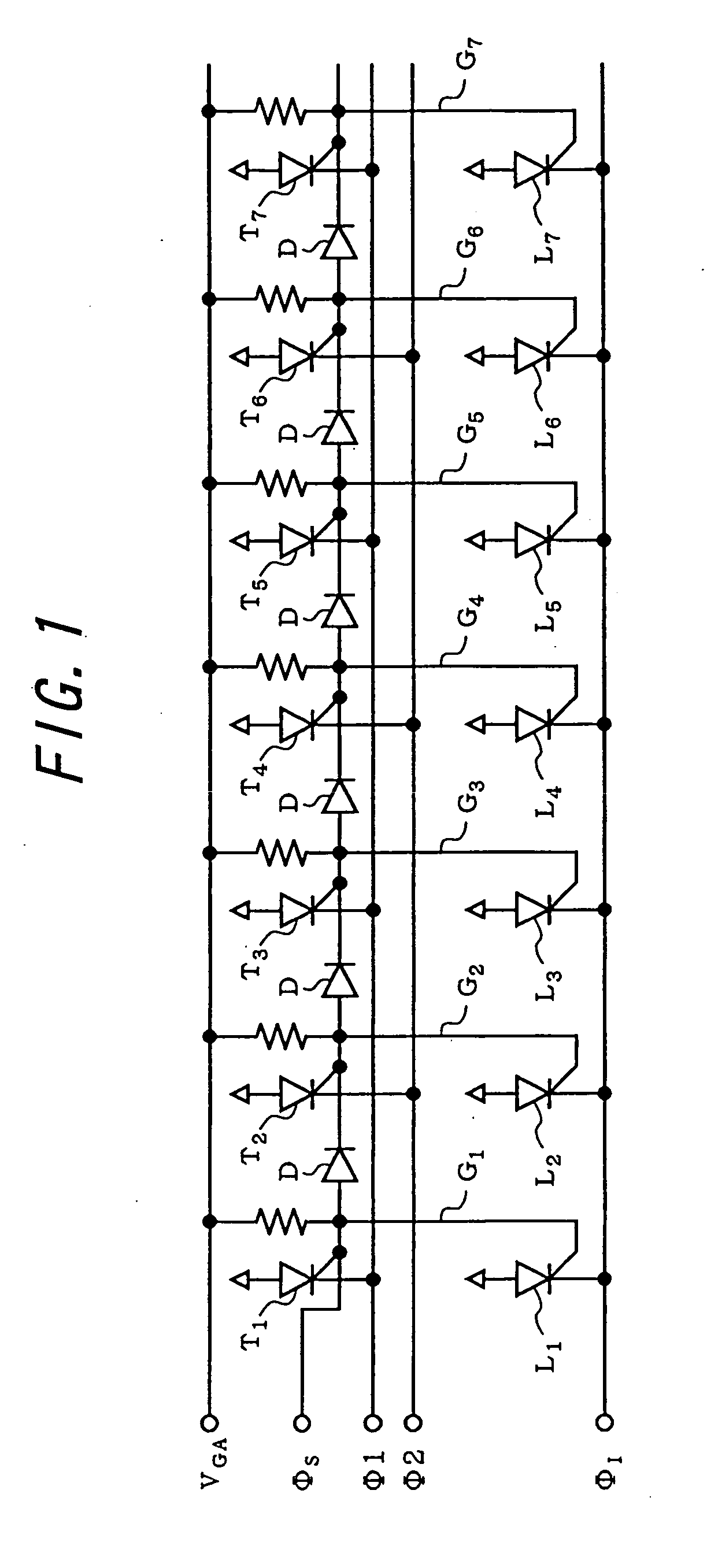
[0066] The present embodiment is directed to a self-scanning light-emitting element array using a schottky barrier diode as a coupling diode. FIG. 6 shows a circuit diagram of the self-scanning light-emitting element array, which is the same as the circuit diagaram in FIG. 1 except that the coupling diode D is replaced by a schottky barrier diode SB.

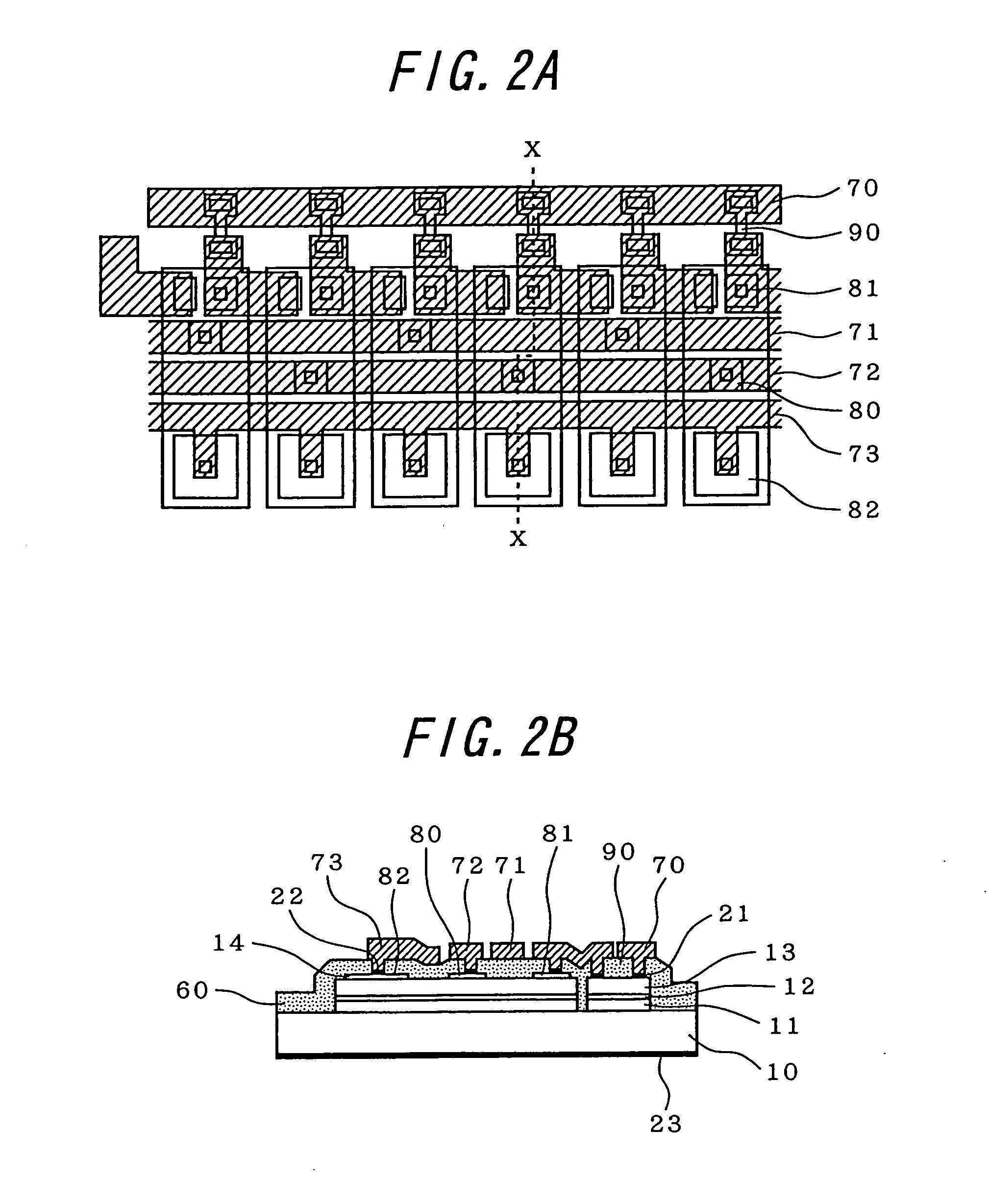
[0067] Referring to FIGS. 7A and 7B, there is shown a device structure of the diode-coupling self-scanning light-emitting element array formed in a chip. FIG. 7A is a plan view and FIG. 7B is a cross-sectional view taken along X-X line in FIG. 7A. On a P-type GaAS substrate 10, there are stacked a P-type AlGaAs epitaxial layer 11, a N-type AlGaAs epitaxial layer 12, a P-type AlGaAs epitaxial layer 13, and a N-type AlGaAs epitaxial layer 14 in this order to form a PNPN-structure. A light-emitting thyristor is fabricated using the PNPN-structure.

[0068] In the figures, reference numeral 21 designates an ohmic electrode for the P-type AlGa...

embodiment 3

[0070] The present embodiment is directed to a self-scanning light-emitting element array in which the start pulse φS terminal is deleted in the self-scanning light-emitting element array of the embodiment 2, thereby decreasing the number of bonding pads on a chip. In the circuit of FIG. 6, the start pulse terminal φS is deleted, and then the function thereof is realized by the clock pulse terminal φ2.

[0071]FIG. 8 shows a circuit diagram of this embodiment. In this case, the gate of the switch element T1 is connected to the clock pulse terminal φ2 via a schottky barrier diode 91 for forming a start pulse. The clock pulse φ2 is supplied to the gate of the switch element T1 as a start pulse via the diode 91.

[0072] The self-scanning light-emitting element array uses a schottky barrier diode as a coupling diode in the same way as the embodiment 2, so that the operation by lower power supply voltage may be realized.


PUM


Abstract

A light-emitting element including a light-emitting thyristor and a schottky barrier diode is provided. A schottky barrier diode is formed by contacting a metal terminal to a gate layer of a three-terminal light-emitting thyristor consisting of a PNPN-structure. A self-scanning light-emitting element array may be driven at 3.0 V by using such a schottky barrier diode as a coupling diode of a diode-coupled self-scanning light-emitting element array.

Description

TECHNICAL FIELD [0001] The present invention generally relates to a light-emitting element and light-emitting element array having a PNPN-structure, particularly to a light-emitting element and light-emitting element array having a logical function. The present invention further relates to a light-emitting element array which is operated at 3.0 volts (V). BACKGROUND ART [0002] A digital circuit has a tendency to decrease its power supply voltage for the requirements of higher speed and lower consumed power. The power supply voltage thereof has been changing from a 5V system to a 3.3V system and further to a lower voltage system. An error of ±10% is allowed for a power supply voltage of 3.3V, therefore a digital circuit should be guaranteed to be operated at 3.0V. [0003] As an example of a digital circuit, a light-emitting element array may be considered. The light-emitting element array in which a number of light-emitting elements are integrated in the same substrate is used for a w...

Claims


Application Information

Patent Timeline
IPC IPC(8): H01L33/40H03K19/14H01L33/08H03K19/177B41J2/44B41J2/455H01L33/30H01L33/00H01L27/15B41J2/45H01L29/74
CPCB41J2/45H01L27/15H01L33/0033
Inventor OHNO, SEIJI
Owner FUJIFILM BUSINESS INNOVATION CORP
Why Eureka
Try Eureka