Method of producing electronic circuit and electronic circuit

a technology of electronic circuits and electronic circuits, applied in the direction of conductive pattern formation, instruments, applications, etc., can solve the problems of affecting the production period and cost affecting the design and production of electronic circuit boards, and affecting the quality of electronic circuit boards

Active Publication Date: 2005-10-13
KK TOSHIBA
View PDF17 Cites 4 Cited by
  • Summary
  • Abstract
  • Description
  • Claims
  • Application Information

AI Technical Summary

Benefits of technology

[0014] According to another aspect of the present invention, there is provided an electronic circuit, comprising a first base pattern which is formed on a substrate and consists of at least a first resin and fine metal particles contained in the first resin; a second base pattern which is formed on the substrate and consists of a second resin having wettability with respect to the substrate lower than that of the first resin or a mixture containing a resin and oils and fats, and fine metal particles contained in the second resin or the mixture; a first metal conductor layer which is formed on the first and second base patterns; and a second metal conductor layer which is formed on the first metal conductor layer.
[0015] According to another aspect of the present invention, there is provided an electronic circuit, comprising a substrate which has a circuit forming region and a plating wire forming region having wettability with respect to a resin lower tha

Problems solved by technology

This manufacturing step requires an exposure mask for each layer, involving a great amount of time and cost for its design and production.
Therefore, a change or modification in the circuit

Method used


Image

  • Method of producing electronic circuit and electronic circuit
  • Method of producing electronic circuit and electronic circuit
  • Method of producing electronic circuit and electronic circuit

Examples


first embodiment

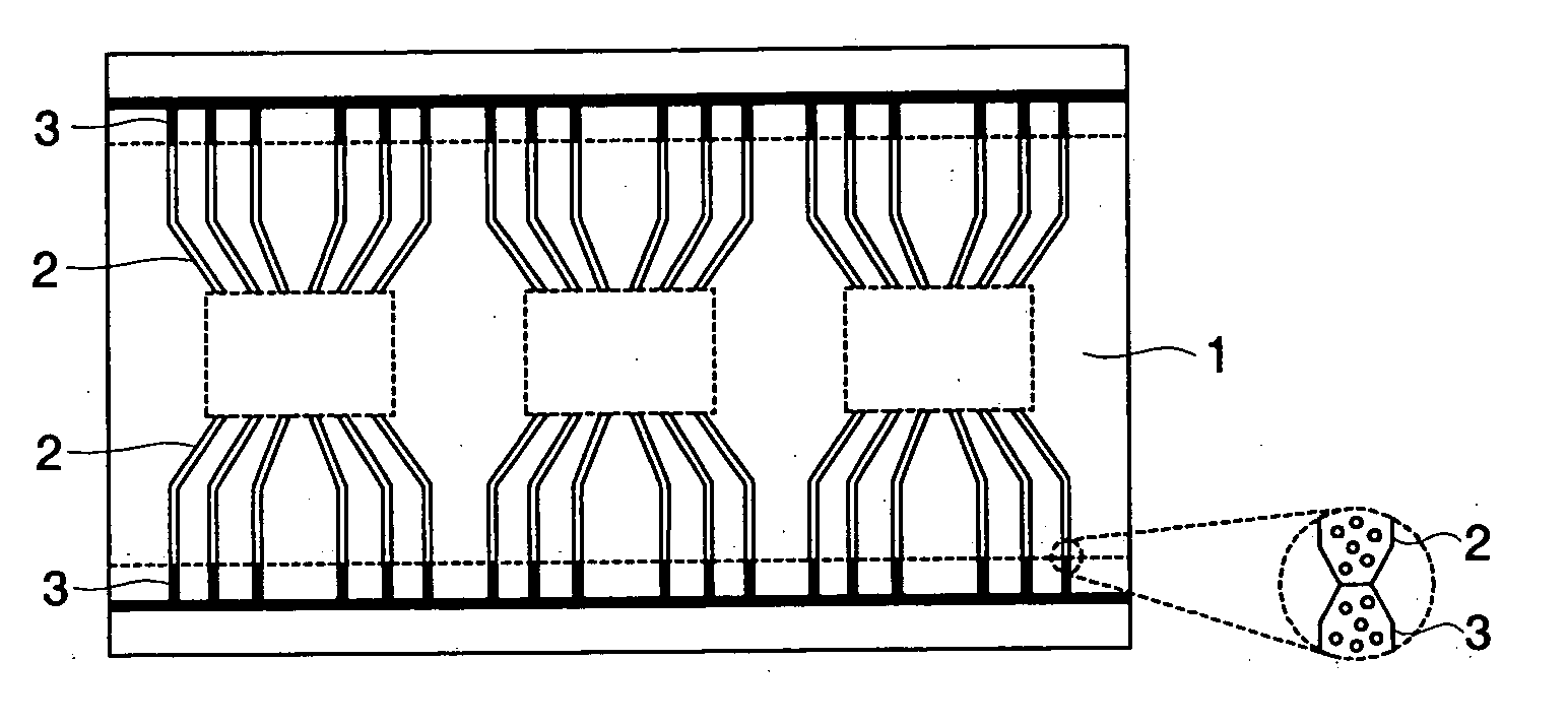
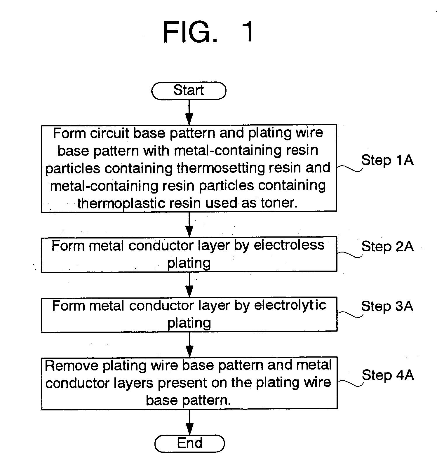
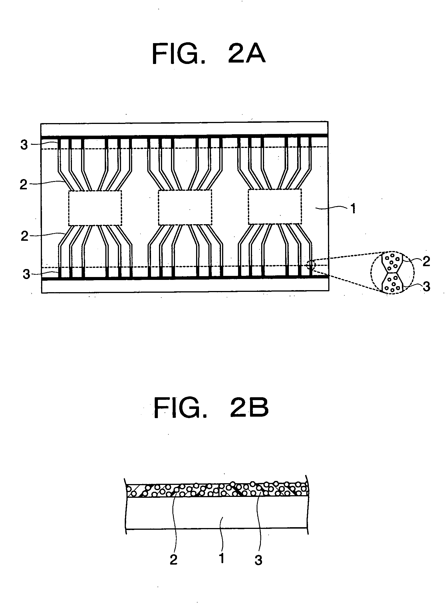
[0033] First Embodiment will be described below. FIG. 1 is a flowchart showing a flow of manufacturing steps for the electronic circuit according to this embodiment. FIG. 2A through FIG. 5B are plan views and vertical sectional views schematically showing manufacturing states of the electronic circuit according to this embodiment. FIG. 6A and FIG. 6B are schematic views of metal-containing resin particles according to this embodiment.

[0034] First, as shown in FIG. 1, FIG. 2A and FIG. 2B, a circuit base pattern 2 (first base pattern) for electroless plating is formed on a substrate 1 using metal-containing resin particles 2A as toner by printing according to electrophotography, and a plating wire base pattern 3 (second base pattern) for electroless plating is formed on the substrate 1 using metal-containing resin particles 3A as toner by printing according to electrophotography (step 1A). Here, the electrophotography is a method by which an electrostatic latent image is formed on th...

second embodiment

[0045] Second Embodiment will be described below. In this embodiment, an example that a resin having wettability with respect to a substrate lower than that of the resin for metal-containing resin particles for forming a circuit base pattern or a mixture of a resin with oils and fats is used as a constituent of metal-containing resin particles for forming a plating wire base pattern will be described. FIG. 7 is a flowchart showing a flow of manufacturing steps for the electronic circuit according to this embodiment, FIG. 8A and FIG. 8B are a plan view and a vertical sectional view schematically showing a manufacturing state of the electronic circuit according to this embodiment, and FIG. 9A and FIG. 9B are schematic views of the metal-containing resin particles according to this embodiment.

[0046] First, as shown in FIG. 7., FIG. 8A and FIG. 8B, a circuit base pattern 2 (first base pattern) for electroless plating is formed on a substrate 1 using metal-containing resin particles 2D ...

third embodiment

[0053] Third Embodiment will be described below. In this embodiment, an example that the circuit forming region of a substrate is undergone a surface roughening treatment and the plating wire forming region of the substrate is coated with a resin having low wettability with respect to a synthetic resin of metal-containing resin particles or a mixture of a resin and oils and fats will be described. FIG. 10 is a flowchart showing a flow of manufacturing steps for the electronic circuit-according to this embodiment, FIG. 11A to FIG. 12B are plan views and vertical sectional views schematically showing manufacturing states of the electronic circuit according to this embodiment, and FIG. 13 is a schematic view of the metal-containing resin particles according to this embodiment.

[0054] First, as shown in FIG. 10, FIG. 11A and FIG. 11B, a circuit forming region 1B which is present around a semiconductor device mounting region 1A of the substrate 1 is undergone a surface roughening treatme...


PUM

PropertyMeasurementUnit
Wettabilityaaaaaaaaaa

Abstract

According to an embodiment of the present invention, a method of producing an electronic circuit comprises printing first metal-containing resin particles which consist of at least a thermosetting resin and fine metal particles and second metal-containing resin particles which consist of at least a thermoplastic resin and fine metal particles by electrophotography to form a first base pattern which consists of the first metal-containing resin particles and a second base pattern which consists of the second metal-containing resin particles on a substrate; forming a first metal conductor layer on the first and second base patterns; forming a second metal conductor layer on the first metal conductor layer by electrolytic plating by supplying electric current to the first metal conductor layer; and removing the second base pattern and the first and second metal conductor layers which are formed on the second base pattern.

Description

CROSS-REFERENCE TO THE INVENTION [0001] This application is based upon and claims the benefit of priority from the prior Japanese Patent Application No. 2004-118122, filed on Apr. 13, 2004; the entire contents of which are incorporated herein by reference. BACKGROUND OF THE INVENTION [0002] 1. Field of the Invention [0003] The present invention relates to a method of producing an electronic circuit and an electronic circuit. [0004] 2. Description of the Related Art [0005] In producing a conventional electronic circuit board, a metal conductor pattern layer is formed on a metal thin film by performing resist application, exposure, development, etching and other processes. This manufacturing step requires an exposure mask for each layer, involving a great amount of time and cost for its design and production. Therefore, a change or modification in the circuit pattern has a large influence on the electronic circuit board production period and cost. [0006] Accordingly, there is develope...

Claims


Application Information

Patent Timeline
IPC IPC(8): H05K3/18H01L21/48H01L23/495H05K1/09H05K3/12H05K3/24
CPCH01L21/4846H05K1/095H05K3/1266H05K3/242H05K3/246H05K2201/0347G03G15/6591Y10S438/951H01L2924/0002H05K2203/0517G03G15/6585G03G15/224H01L2924/00E02B7/42E02B13/02
Inventor AOKI, HIDEOYAMAGUCHI, NAOKOTAKUBO, CHIAKIYAMAUCHI, TOSHIAKIIMAMIYA, KOJIHASHIZUME, HIROSHI
Owner KK TOSHIBA
Why Eureka
Try Eureka