

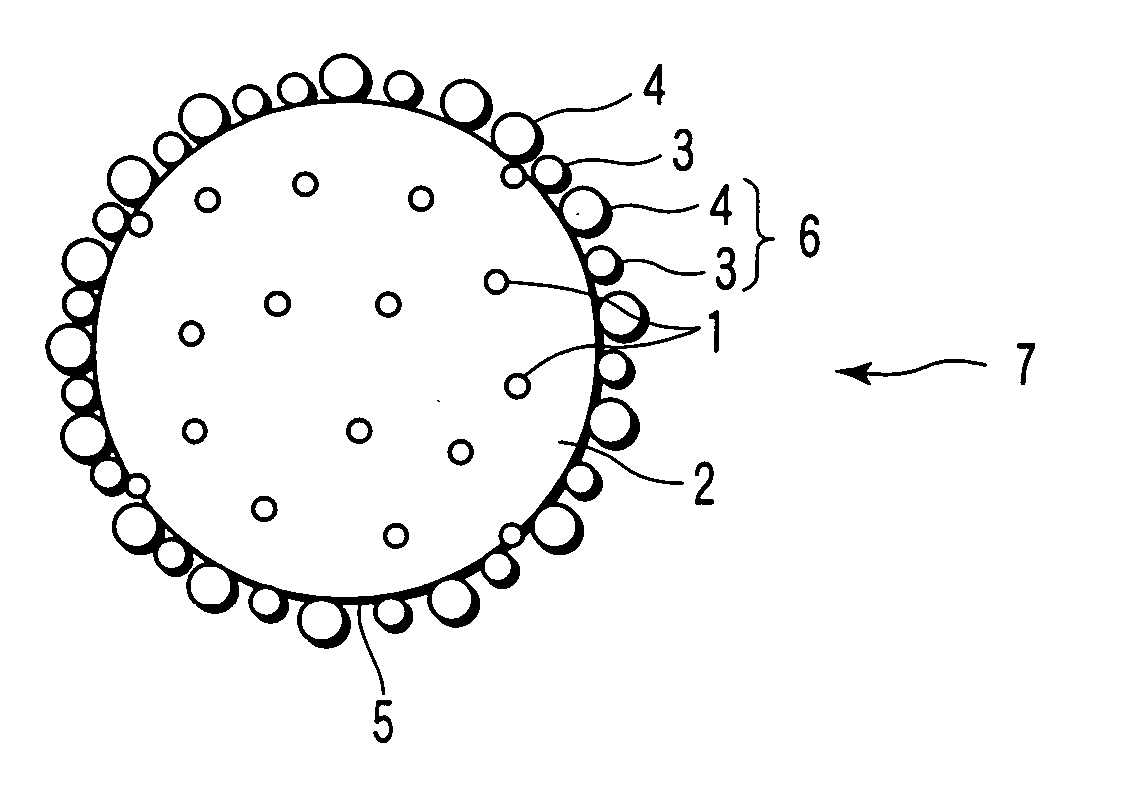
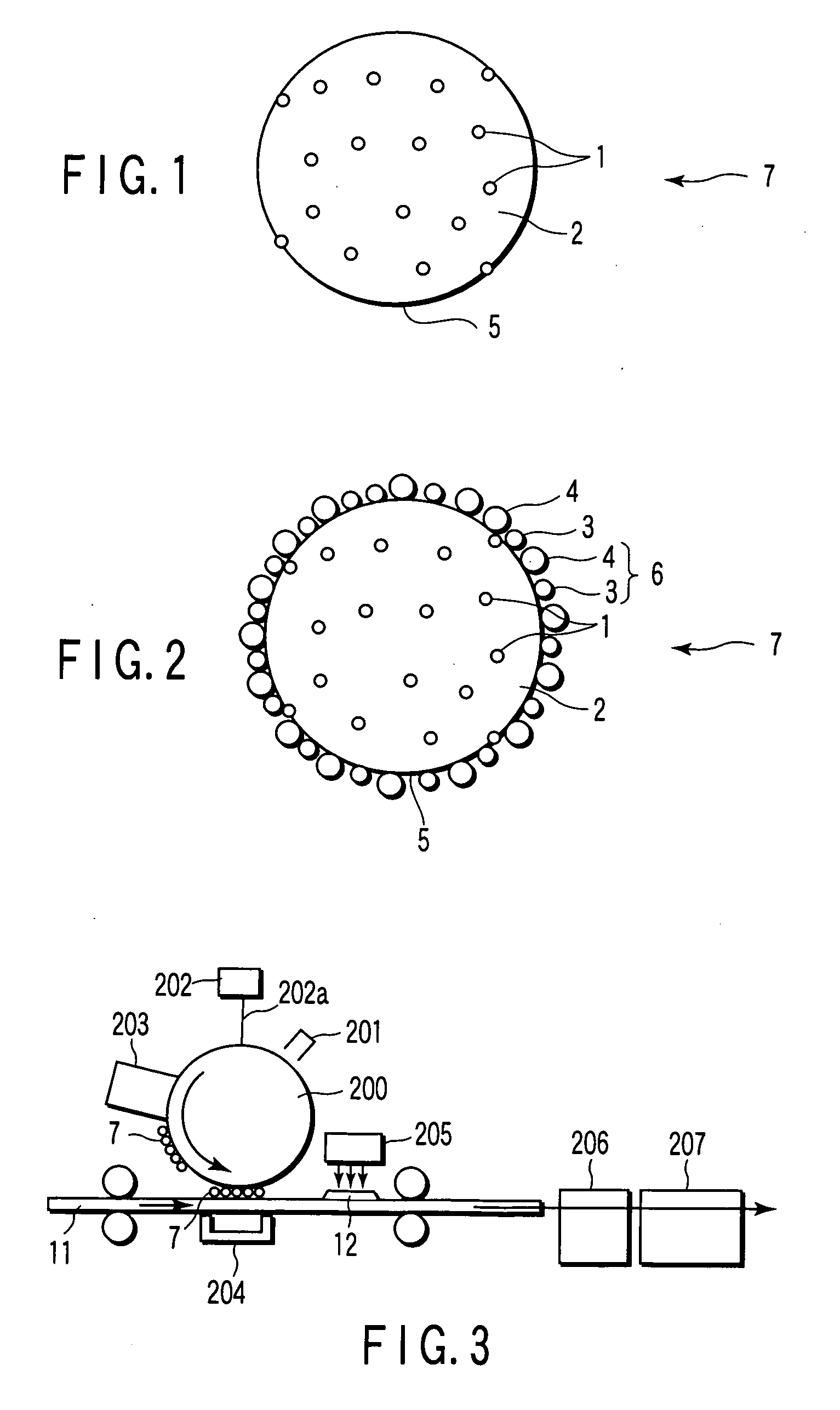
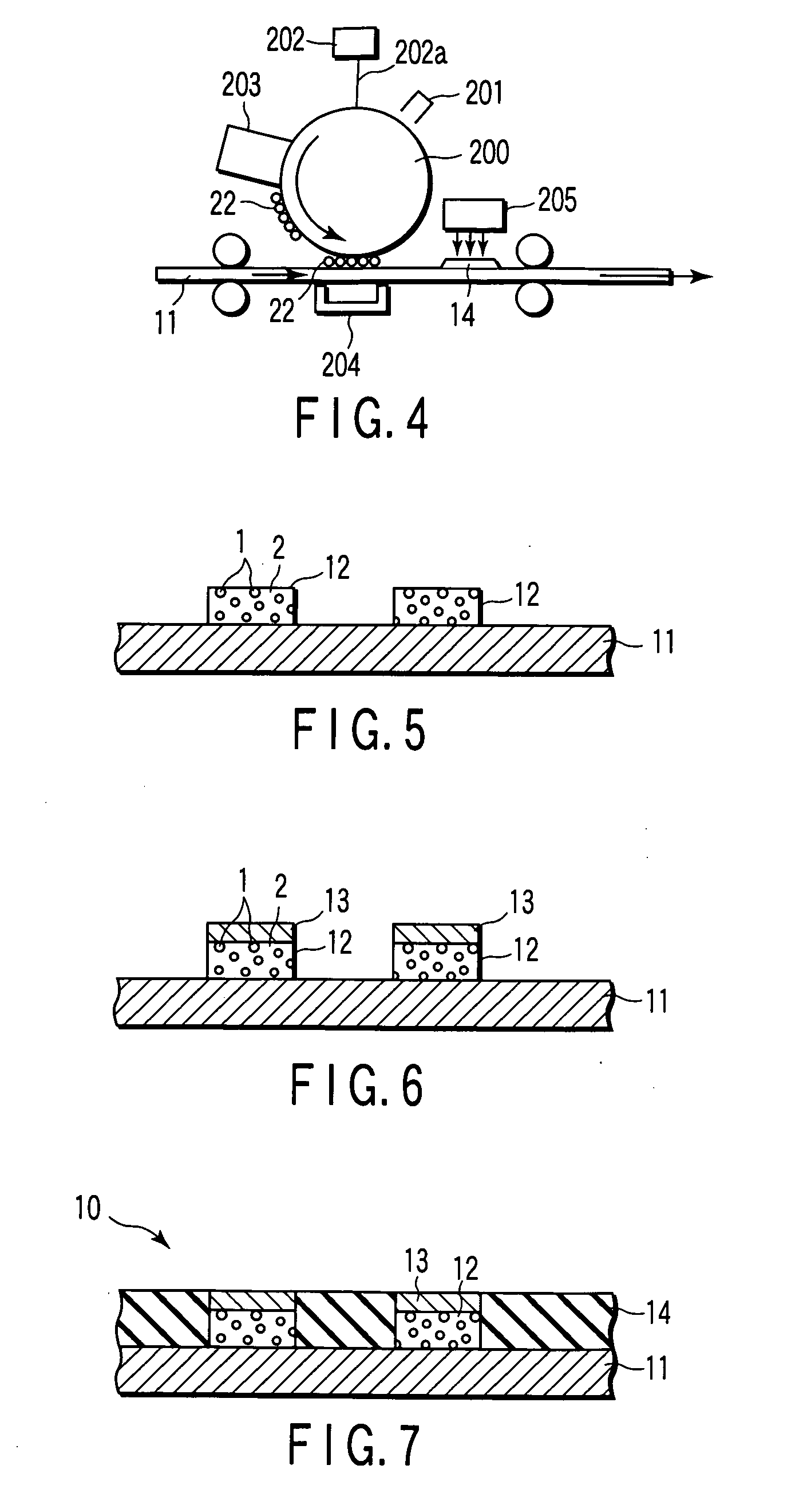
Toner for producing wiring board and method of producing wiring board using thereof
a technology of wiring board and toner, which is applied in the field of toner, can solve the problems of inflexible method, long time-consuming and laborious to produce wiring board masks, and high cost of multi-layered wiring board production, and achieves low cost, stable chargeability, and easy and large-item-small-scale production.
- Summary
- Abstract
- Description
- Claims
- Application Information
AI Technical Summary
Benefits of technology
Problems solved by technology
Method used
Image

Examples
example 1
[0102] A thermosetting epoxy resin 50 part by weight as a binder and copper particles with a volume average particle diameter of 0.6 μm 50 part by weight as conductive particles were evenly mixed by a Henshel mixer for 5 minutes to obtain a mixture. The mixture was kneaded at 90° C. for 10 minutes by a pressurizing kneader for gelation and then quenched to obtain a kneaded product. The obtained kneaded product was coarsely crushed to 2 mm or smaller by a hammer mill. After that, the coarsely crushed particles are pulverized and sieved to about 8.0 μm by I type jet pulverizer and DSX sieving apparatus to obtain toner particles.
[0103] The obtained toner particles 100 part by weight were mixed with silica R 974 (manufactured by Degussa, average particle diameter 12 nm, dimethyldichlorosilane-surface treated) 1 part by weight and silica NAX 50 (manufactured by NIPPON AEROSIL CO., LTD., average particle diameter 35 nm, hexamethyldisilazane-surface treated) 1 part by weight by a Henshel ...
example 2
[0111] A toner was obtained in the same manner as Example 1, except that the pulverization and sieving conditions of the I type jet pulverizer and DSX sieving apparatus were changed.
[0112] The obtained toner was subjected to the particle size distribution measurement similarly to Example 1 to find that the 50% by volume particle diameter was 7.8 μm and the ratio of the fine particles with 4 μm or smaller was 22.0% by number.
[0113] The intrinsic volume resistivity was measured similarly to Example 1 to find it was 4.49×10¹⁰ Ωcm.
[0114] Further, using the obtained toner, similarly to Example 1, a substrate bearing the conductive underlayer and an ordinal paper sample were produced.
[0115] The conductive underlayer pattern of the ordinal paper sample was observed with eyes to find that the line pattern was drawn clearly and excellent with little fogging in non-image parts and little contamination with dust in the peripheral parts of the image.
[0116] Fogging was evaluated based on re...
example 3
[0119] A toner was produced in the same manner as Example 1, except that the addition amounts of the thermosetting epoxy resin and the copper particles with 0.6 μm particle diameter were changed to be 30 part by weight and 70 part by weight, respectively.
[0120] The obtained toner was subjected to the particle size distribution measurement similarly to Example 1 to find that the 50% by volume particle diameter was 8.1 μm and the ratio of the fine particles with 4 μm or smaller was 14.0% by number.
[0121] The intrinsic volume resistivity was measured similarly to Example 1 to find it was 0.8×10¹⁰ Ωcm.
[0122] Further, using the obtained toner, similarly to Example 1, a substrate bearing the conductive underlayer and an ordinal paper sample were produced.
[0123] The conductive underlayer pattern of the ordinal paper sample was observed with eyes to find that the line pattern was drawn clearly and excellent with little fogging in non-image parts and little contamination with dust in the...
PUM
| Property | Measurement | Unit |
|---|---|---|
| size | aaaaa | aaaaa |
| particle diameter | aaaaa | aaaaa |
| particle diameter | aaaaa | aaaaa |
Abstract
Description
Claims
Application Information