
Macro cell for integrated circuit physical layer interface

a physical layer interface and micro cell technology, applied in the field of micro cells for integrated circuit physical layer interfaces, can solve the problems of difficult timing closure, time-consuming, and crucial skew between data and clock strobe signals,

Active Publication Date: 2005-10-13
BELL SEMICON LLC
View PDF11 Cites 57 Cited by
  • Summary
  • Abstract
  • Description
  • Claims
  • Application Information

AI Technical Summary

Problems solved by technology

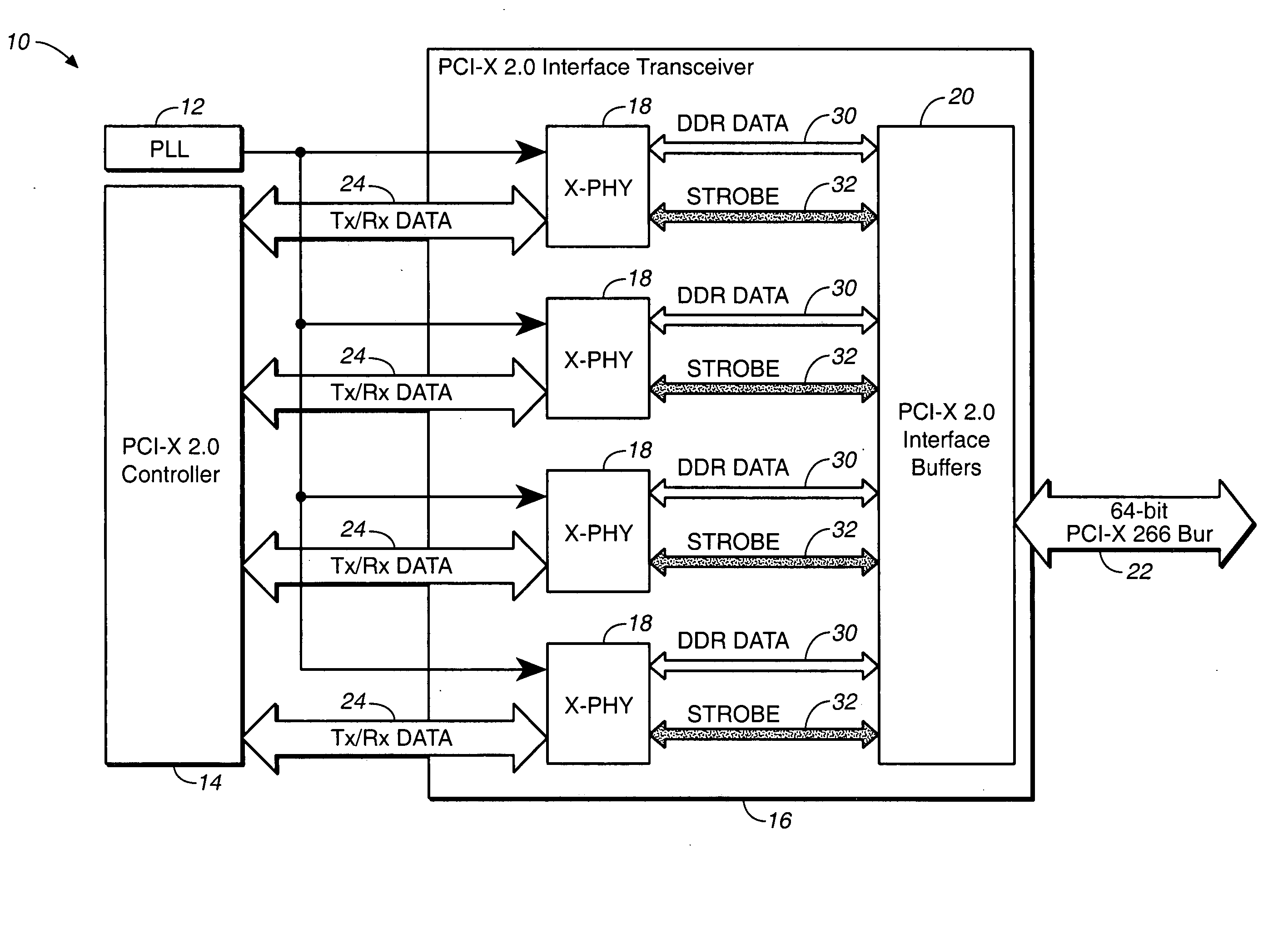
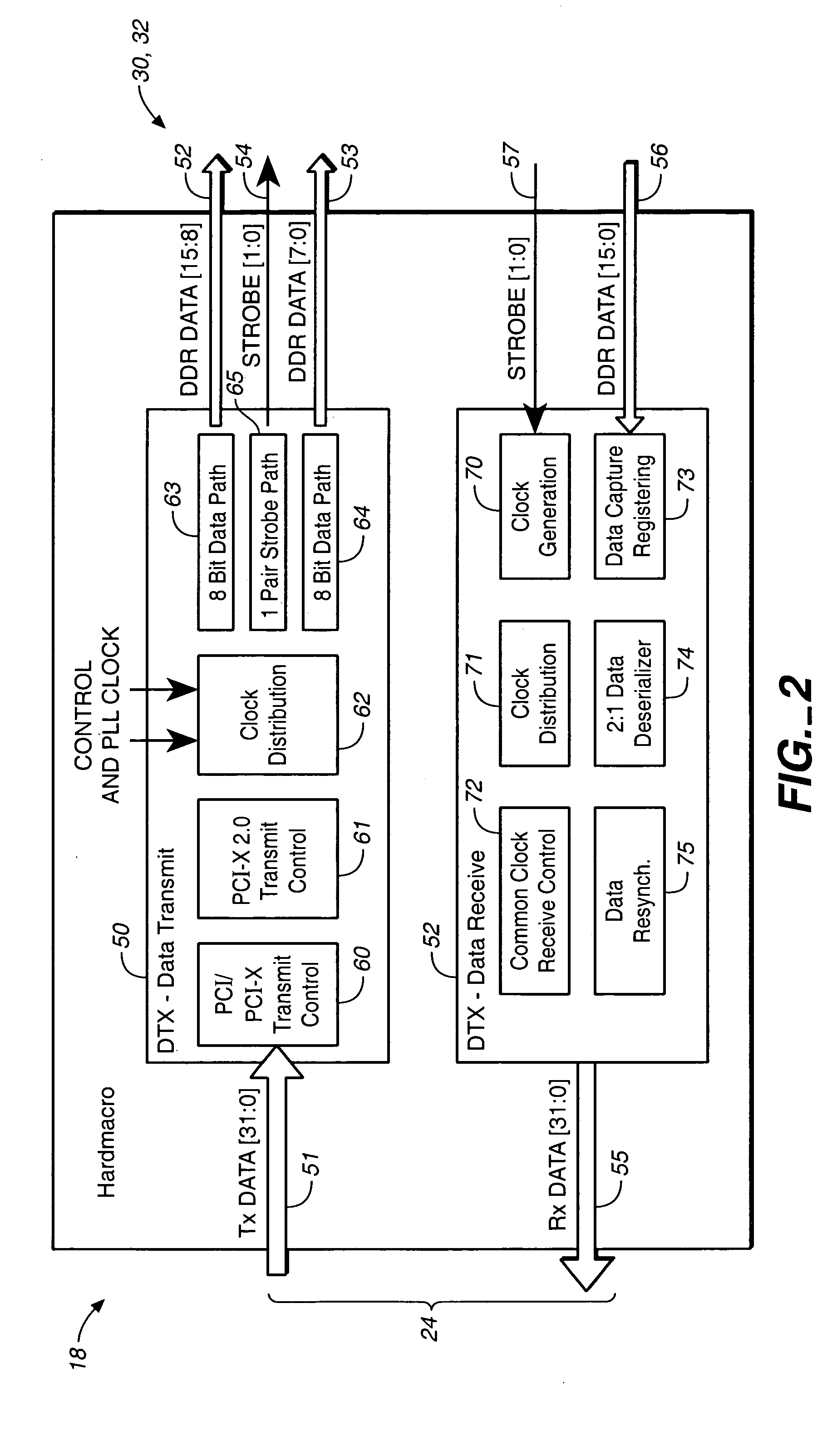
The timing requirements for a PCI-X 2.0 PHY interface are challenging.
With these higher transfer speeds, the skew between the data and the clock strobe signal becomes crucial.
Therefore, timing closure for such a physical layer interface can be difficult and time consuming.
This work is thus a time consuming process due to the manual and iterative steps involved.

Method used


Image

  • Macro cell for integrated circuit physical layer interface
  • Macro cell for integrated circuit physical layer interface
  • Macro cell for integrated circuit physical layer interface

Examples


Embodiment Construction

[0024] Semiconductor integrated circuits are traditionally designed and fabricated by first preparing a schematic diagram or hardware description language (HDL) specification of a logical circuit in which functional elements are interconnect to perform a logical function. For example, with standard cell technology, the schematic diagram or HDL specification is synthesized into standard cells of a specific cell library. Each cell corresponds to a logical function unit, which is implemented by one or more transistors that are optimized for the cell. The cells in the cell library are defined by cell definitions. Each cell library definition includes a cell layout definition and cell characteristics. The cell layout definition includes a predetermined layout pattern for the transistors in the cell, geometry data for the cell's transistors and cell routing data.

[0025] These cells can correspond to low-level functions, such as logical “AND”, “OR”, “NOR gates or higher-level functions suc...


PUM


Abstract

A macro cell is provided for an integrated circuit design having an input-output (IO) region with a plurality of IO buffer cells physically dispersed with other cells in IO slots along an interface portion of the IO region. The macro cell includes a plurality of macro cell IO signal slots that are physically dispersed so as to substantially align with the IO buffer cells in the interface portion. The macro cell also includes an interface definition having a plurality of interface IO signal nets, which are routed to corresponding ones of the plurality of macro cell signal slots. The macro cell is adapted to be instantiated as a unit in the integrated circuit design.

Description

FIELD OF THE INVENTION [0001] The present invention relates to semiconductor integrated circuits and, more particularly, to hard macro cells that can be instantiated in an integrated circuit design for driving a physical layer interface. BACKGROUND OF THE INVENTION [0002] Physical layer (PHY) interface devices are used on integrated circuits for communicating with external devices, such as other integrated circuits, typically through a data bus or a set of signal wires. The physical layer device is typically configured to implement a desired communication protocol or specification that has been established for the particular interface. For example, the Peripheral Component Interconnect (PCI) bus specification is an industry standard specification for high-performance input-output (IO) interconnections for transferring data between a CPU and its peripherals. As versions of these standards change over time to achieve greater performance, the demands on the physical layer interface dev...

Claims


Application Information

Patent Timeline
IPC IPC(8): G06F17/50
CPCG06F17/5045G06F30/30
Inventor BUTT, DERRICK SAI TANGCOCHRANE, BRUCE C.SETO, HUI YINLAU, WILLIAM W.MCCARTHY, THOMAS E.
Owner BELL SEMICON LLC
Learn More