Apparatus for thermal treatment of substrates

a substrate and apparatus technology, applied in the direction of chemically reactive gases, coatings, crystal growth processes, etc., can solve the problems of high cost of integrated circuit manufacturers, wafer handlers, and more vulnerable to physical damage, so as to facilitate conductive cooling of substrates and reduce the time of cooling. time, the effect of significantly faster cooling of substrates

Inactive Publication Date: 2005-10-20
RAAIJMAKERS IVO
View PDF38 Cites 247 Cited by
  • Summary
  • Abstract
  • Description
  • Claims
  • Application Information

AI Technical Summary

Benefits of technology

[0014] Advantageously, the illustrated embodiments facilitate conductively cooling a substrate, thus cooling the substrate significantly faster than by radiation alone. As the cooling methods and mechanisms do not require handling the substrate with a pick-up device, down time (specifically that caused by waiting for substrate to reach a temperature at which it can be safely handled) is significantly reduced. Additionally, the substrat

Problems solved by technology

For example, in an epitaxial silicon deposition reactor, processing temperatures in the reaction chamber are typically in the range of 1,000-1,200° C., while the maximum temperature that the robotic wafer handler can handle is only about 900° C. Furthermore, at high temperatures, the wafer is more vulnerable to physical damage which c

Method used


Image

  • Apparatus for thermal treatment of substrates
  • Apparatus for thermal treatment of substrates
  • Apparatus for thermal treatment of substrates

Examples


Embodiment Construction

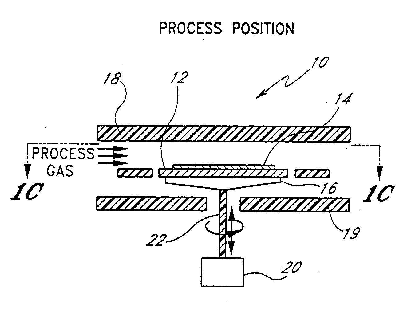
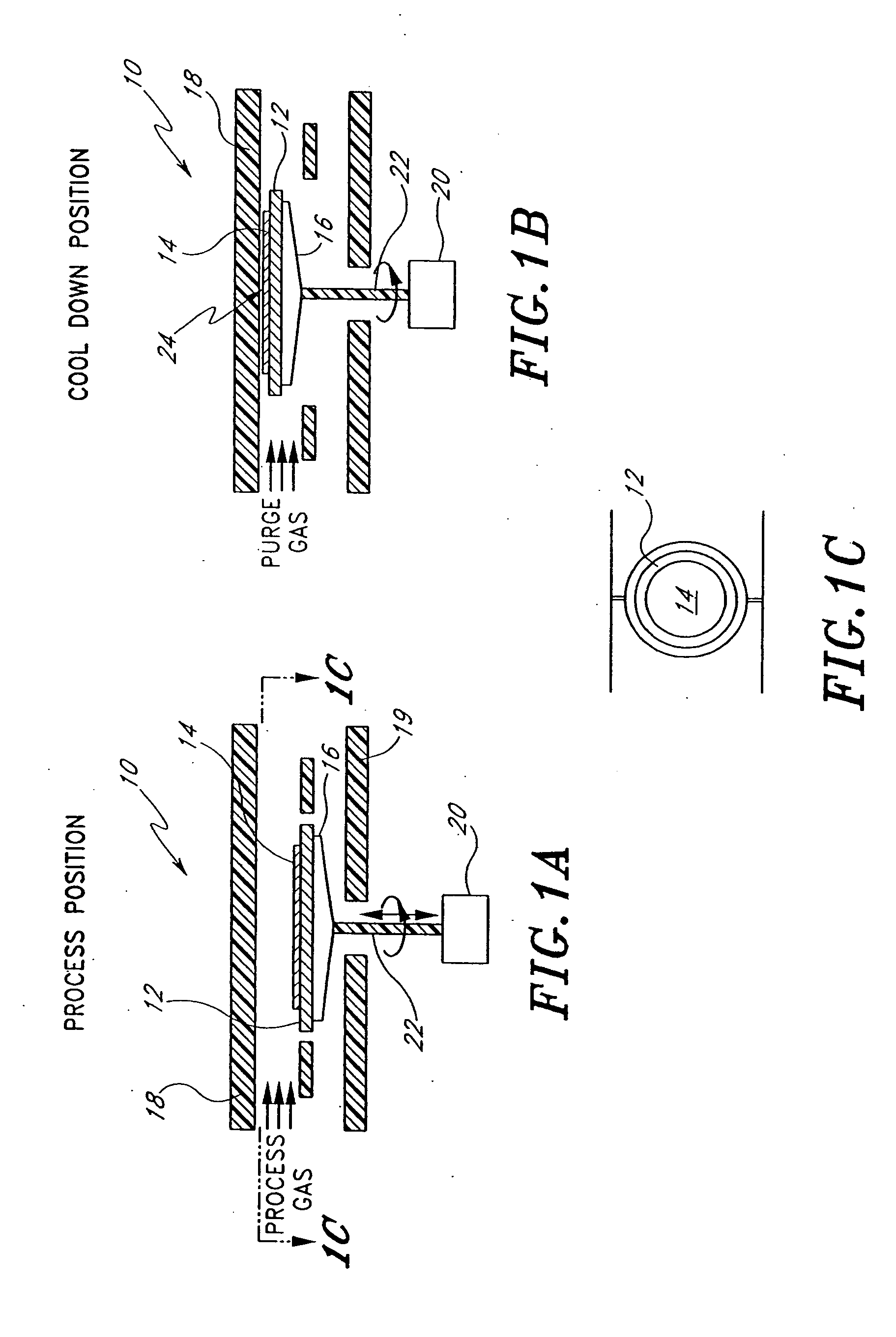
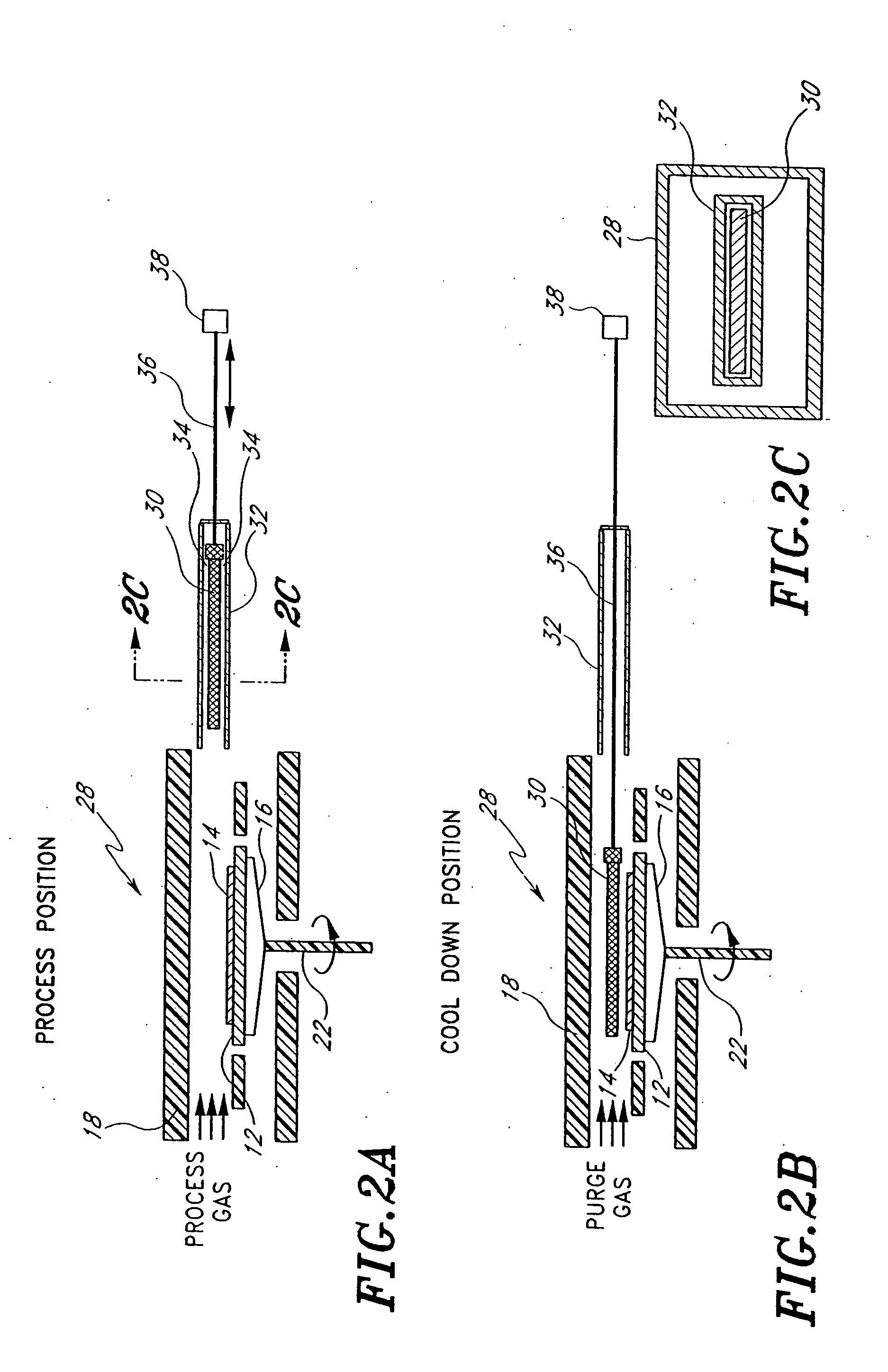
[0025] While the invention is illustrated in the context of a single-wafer, horizontal gas flow reactor, it will be understood by one of ordinary skill in the art that the cooling mechanism of the present invention is not limited to any specific type of reactors or processing chambers. Rather, the skilled artisan will find application for the principles disclosed herein in connection with a number of different types of processing chambers or reactors, including cluster tools, batch processing systems, vertical gas flow or showerhead systems, etc. Furthermore, while the applications have particular utility for cooling down wafers before handling and removing the wafer from the process chamber, the principles disclosed herein have application whenever it is desirable to cool a workpiece prior to handling or storage.

[0026]FIGS. 1A, 1B and 1C illustrate a processing chamber which incorporates a cooling system constructed in accordance with a first preferred embodiment of the present in...


PUM

PropertyMeasurementUnit
Temperatureaaaaaaaaaa
Lengthaaaaaaaaaa

Abstract

Methods and apparatuses are provided for cooling semiconductor substrates prior to handling. In one embodiment, a substrate and support structure combination is lifted after high temperature processing to a cold wall of a thermal processing chamber, which acts as a heat sink. Conductive heat transfer across a small gap from the substrate to the heat sink speeds wafer cooling prior to handling the wafer (e.g., with a robot). In another embodiment, a separate plate is kept cool within a pocket during processing, and is moved close to the substrate and support after processing. In yet another embodiment, a cooling station between a processing chamber and a storage cassette includes two movable cold plates, which are movable to positions closely spaced on either side of the wafer.

Description

CROSS-REFERENCE TO RELATED APPLICATIONS [0001] This application is a continuation of U.S. patent application Ser. No. 09 / 584,656, filed May 30, 2000, which is a continuation of U.S. patent application Ser. No. 09 / 150,986, filed Sep. 10, 1998 (now U.S. Pat. No. 6,108,937).BACKGROUND OF THE INVENTION [0002] This invention relates to methods and devices for cooling bodies such as semiconductor substrates after they are heated. More particularly, the invention relates to cooling a substrate by heat transfer between the substrate and a heat sink prior to handling the substrate. [0003] Semiconductor wafers or other such substrates are subjected to very high treatment or processing temperatures. For example, in certain chemical vapor deposition (CVD) processes, the temperatures can approach 1,200° C. In a typical cycle, a wafer is transferred from a room temperature cassette by a robotic wafer handler into a processing or reaction chamber, where it is subjected to a high temperature treatm...

Claims


Application Information

Patent Timeline
IPC IPC(8): C23C16/44C23C16/54C23C16/56C30B25/10H01L21/00H01L21/205
CPCC23C16/54H01L21/67109C30B25/10C23C16/56H01L21/02
Inventor RAAIJMAKERS, IVO
Owner RAAIJMAKERS IVO
Why Eureka
Try Eureka