Semiconductor device, method for producing the same, circuit board, and electronic apparatus

a semiconductor and semiconductor technology, applied in the direction of semiconductor/solid-state device details, semiconductor devices, electrical devices, etc., can solve the problems of substrate warpage, difficult mounting of semiconductor chips on wiring boards, and difficult stacking of semiconductor chips, so as to reduce the internal stress or thermal expansion coefficient of the insulating layer acting on the substrate, reduce the internal stress or thermal expansion coefficient of the insulating layer, and reduce the effect of substrate warpag

Inactive Publication Date: 2005-10-20
SEIKO EPSON CORP
View PDF5 Cites 16 Cited by
  • Summary
  • Abstract
  • Description
  • Claims
  • Application Information

AI Technical Summary

Benefits of technology

[0009] An advantage of the invention is to provide a semiconductor device in which the warpage of substrates caused by the difference in stress between the substrates and functional layers formed on the substrates is eliminated or minimized, and a method for making the semiconductor device. A circuit board and an electronic apparatus incorporating the semiconductor device are also provided.
[0010] An aspect of the invention provides a method for making a semiconductor device having an electrode penetrating a substrate. The method includes (a) forming a concavity in an active face of the substrate; (b) forming an insulating layer on the active face of the substrate and the interior of the concavity; (c) removing at least part of the insulating layer formed outside the concavity; (d) forming the electrode by filling the interior of the concavity with a conductor; and (e) exposing the electrode from a rear face of the substrate opposite to the active face by milling the substrate from the rear face side. The steps (a) to (e) are performed in that order.
[0011] According to this method, the internal stress or thermal expansion coefficient of the insulating layer can be eliminated or minimized during the process of removing the insulating layer on the active face of the substrate. Thus, the internal stress or thermal expansion coefficient of the insulating layer acting upon the substrate can be eliminated or minimized. The difference in internal stress or thermal expansion coefficient between the substrate and the insulating layer can also be reduced. Thus, warpage of the substrate can be prevented. When a plurality of the semiconductor devices are stacked, an adhesive free of conductive particles, a reinforcing member, or the like is placed between the adjacent semiconductor devices to ensure insulation between the semiconductor devices. Thus, even when the insulating layer formed on the active face of the substrate is removed, troubles will not occur because of the adhesive or the like having an insulating function.
[0012] In the step (c) above, the insulating layer may be etched while covering the concavity with a mask to protect the insulating layer inside the concavity from an etchant. In this manner, it becomes possible to prevent removal of the insulating layer inside the concavity.
[0013] In step (c), the entire face of the insulating layer may be etched while adjusting the etching rate of the insulating layer formed on the substrate to be higher than the etching rate of the insulating layer formed on the interior of the concavity in the substrate. In this manner, the insulating layers on the substrate can be removed without affecting the insulating layer inside the concavity. Moreover, since a step of forming a mask is no longer necessary, the process is simple, and the time required for production can be reduced.
[0014] Another aspect of the invention provides a method for making a semiconductor device having an electrode penetrating a substrate. The method includes (f) forming a concavity in an active face of the substrate; (g) forming an insulating layer on the active face of the substrate and interior of the concavity; (h) forming the electrode by filling the interior of the concavity with a conductor; (i) removing at least a portion of the insulating layer outside the concavity; and (j) exposing the electrode from a rear face of the substrate opposite to the active face by milling the substrate from the rear face side. In this method, the steps (f) to (j) are performed in that order.

Problems solved by technology

As a result, the substrates deform and warp due to the stress.
The warpage in the substrates makes it difficult to mount the semiconductor chips on a wiring board or the like.
Thus, sometimes it is difficult to stack the semiconductor chips and to provide electrical or mechanical interconnection between the semiconductor chips and the electrodes.

Method used


Image

  • Semiconductor device, method for producing the same, circuit board, and electronic apparatus
  • Semiconductor device, method for producing the same, circuit board, and electronic apparatus
  • Semiconductor device, method for producing the same, circuit board, and electronic apparatus

Examples


first embodiment

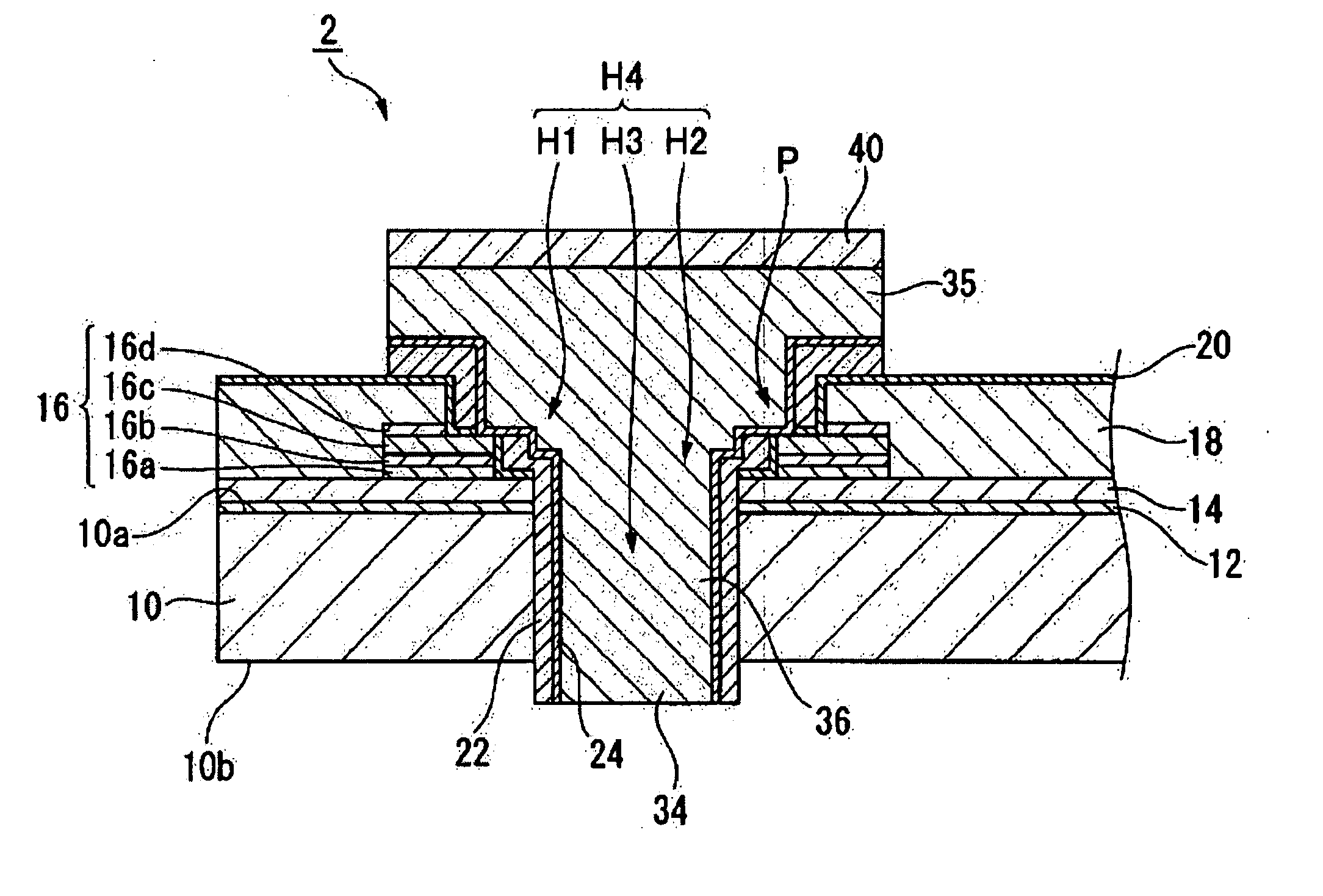
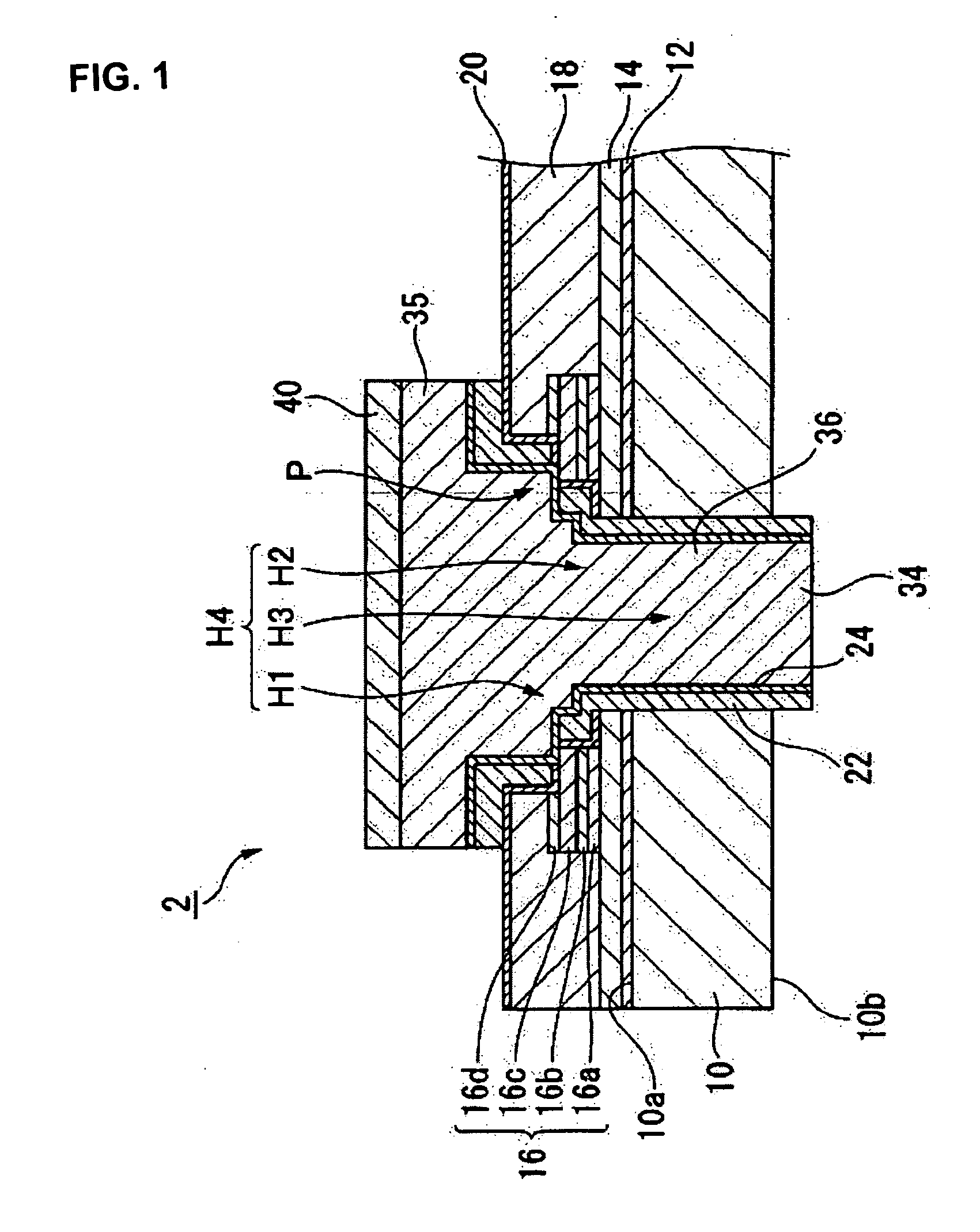
[0038] A semiconductor chip, which is a semiconductor device according to a first embodiment of the invention, will first described with reference to FIG. 1. FIG. 1 is a side cross-sectional view of an electrode of a semiconductor chip 2 according to the first embodiment. The semiconductor chip 2 includes a substrate 10 in which an integral circuit is formed, and an electrode 34. The electrode 34 is formed in a through hole H4 across an active face 10a and the rear face 10b of the substrate 10. A first insulating film 22 is disposed between the electrode 34 and the inner wall of the through hole H4.

[Semiconductor Device]

[0039] The semiconductor chip 2 shown in FIG. 1 has an integral circuit (not shown) constituted from electronic devices such as transistors, memory devices, and the like, on the surface 10a of the substrate 10 composed of silicon and the like. On the active face 10a of the substrate 10, an insulating film 12 composed of silicon oxide (SiO2) or the like is disposed....

second embodiment

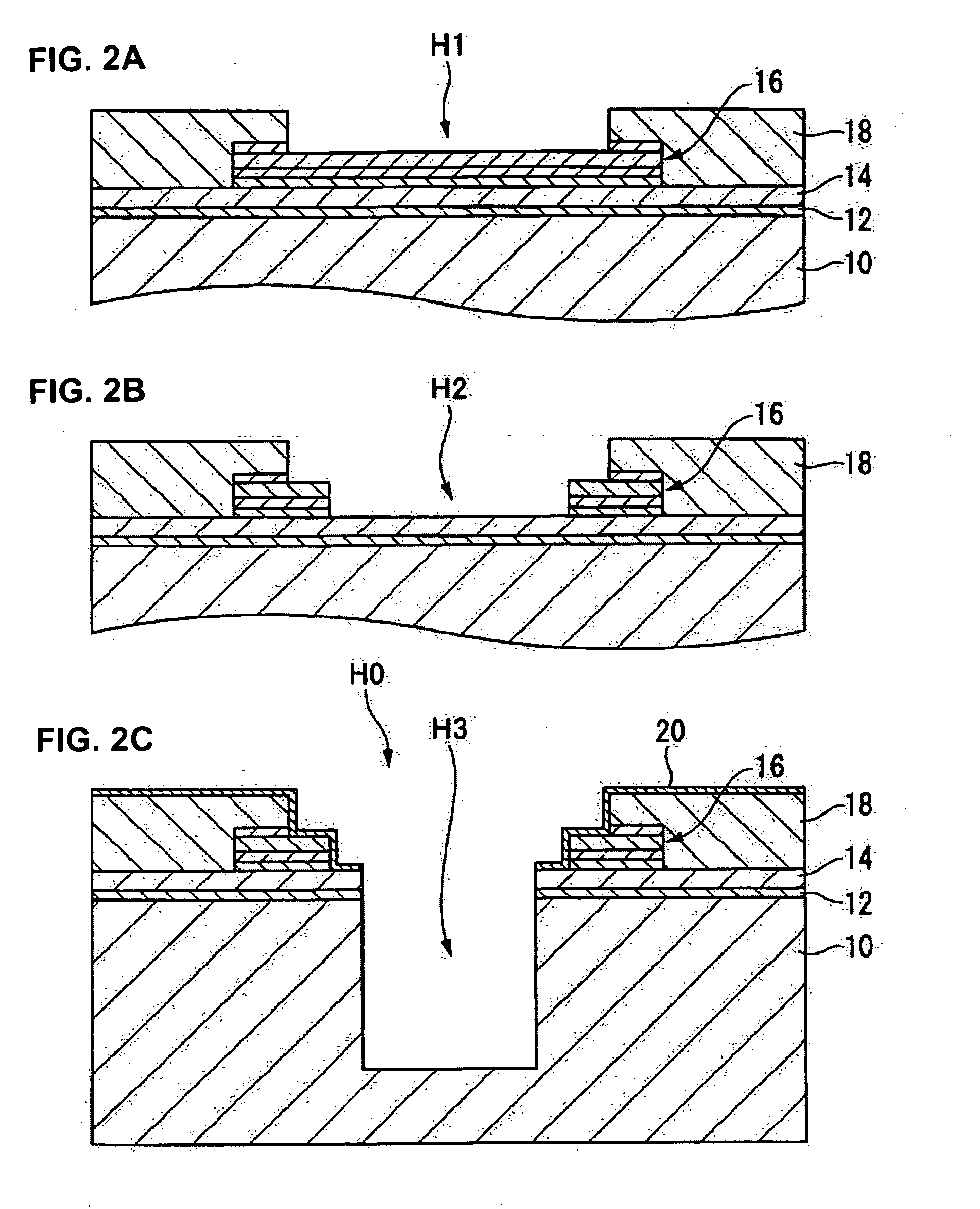
[0081] In the first embodiment, the first insulating film 22 is etched before the electrode 34 is formed in the concavity H0. In the second embodiment, the first insulating film 22 is etched after the electrode 34 is formed in the concavity H0. The second embodiment will now be described with reference to the drawings. The descriptions of the steps identical to the first embodiment are omitted to avoid redundancy.

[0082] The first insulating film 22 is formed on the substrate 10 by the steps shown in FIGS. 2A to 3A. Then, the base film 24 is formed to cover the surface of the electrode pad 16 and the first insulating film 22, as shown in FIG. 12A. Thus, this embodiment differs from the first embodiment in which the first insulating film 22 is etched before the formation of the base film 24. In the second embodiment, the base film 24 is formed by the same technique as described in the first embodiment.

[0083] Next, the electrode 34 shown in FIG. 12B is formed. In particular, a resist...


PUM


Abstract

A method for making a semiconductor device having an electrode penetrating a substrate includes (a) forming a concavity in an active face of the substrate; (b) forming an insulating layer on the active face of the substrate and the interior of the concavity; (c) removing at least part of the insulating layer formed outside the concavity; (d) forming the electrode by filling the interior of the concavity with a conductor; and (e) exposing the electrode from a rear face of the substrate opposite to the active face by milling the substrate from the rear face side. In this method, (a) to (e) are performed in that order.

Description

RELATED APPLICATIONS [0001] This application claims priority to Japanese Patent Application No. 2004-121646 filed Apr. 16, 2004 which is hereby expressly incorporated by reference herein in its entirety. BACKGROUND OF THE INVENTION [0002] 1. Technical Field [0003] The present invention relates to semiconductor devices, methods for making the semiconductor devices, circuit boards, and electronic apparatuses. [0004] 2. Related Art [0005] Demands for smaller, light-weight portable electronic apparatuses, such as cellular phones, portable personal computers, and personal data assistances (PDAs), also require various electronic components in these apparatuses to achieve size reduction. For example, the technique of packaging semiconductor chips has been improved, and now an ultra compact packaging technique called chip scale packaging (CSP) is available. Semiconductor chips produced by the CSP technique achieves high-density mounting since the mount area is about the same as the area of ...

Claims


Application Information

Patent Timeline
Patent Type & Authority Applications(United States)
IPC IPC(8): H01L23/52H01L21/3205H01L21/60H01L21/768H01L23/12H01L23/48H01L25/00H01L25/065H01L25/07H01L25/18H01L27/01
CPCH01L21/76898H01L23/481H01L25/0657H01L2224/16145H01L2225/06513H01L2225/06541H01L2924/15311H01L25/50H01L24/05H01L24/11H01L24/13H01L2224/02372H01L2224/02381H01L2224/05001H01L2224/05009H01L2224/05023H01L2224/05024H01L2224/05025H01L2224/05147H01L2224/05184H01L2224/05548H01L2224/13009H01L2924/00014H01L2224/05599
Inventor MIYAZAWA, IKUYA
Owner SEIKO EPSON CORP
Why Eureka
Try Eureka