Semiconductor integrated circuit and a burn-in method thereof

a technology of integrated circuit and integrated circuit, which is applied in the direction of logic circuit coupling/interface arrangement, pulse technique, instruments, etc., can solve the problem of not being paid to delay, the output operation delay due to the level shifting function, and the increase in the speed of external output operation synchronized with a clock signal, so as to reduce the propagation delay of latch data to the external output buffer

Inactive Publication Date: 2005-10-20
RENESAS ELECTRONICS CORP
View PDF10 Cites 5 Cited by
  • Summary
  • Abstract
  • Description
  • Claims
  • Application Information

AI Technical Summary

Benefits of technology

[0027] The latch circuit receives a clock signal from the outside and performs an output latch operation, thereby enabling an influence of the internal clock delay in output operation synchronized with an external clock signal to be reduced.
[0028] When the latch circuit is disposed close to the external output buffer, the propagation delay of latch data to the external output buffer can be reduced.

Problems solved by technology

In the conventional techniques, however, attention is not paid to delay in the output operation due to the level shifting function and, further, delay in external output operation due to propagation delay in a clock signal with respect to the point of addressing increase in the speed of external output operation synchronized with a clock signal.
First, the output operation delay due to the level shifting function was examined.
However, the inventors herein have found that delay in a data output timing from an external clock signal is increased by the output operation delay due to the level shift circuit and the propagation delay of the internal clock.
However, a sufficient voltage stress cannot be put on a MOS transistor having a high breakdown voltage, so that an initial failure cannot be found, and the possibility that the failure becomes apparent in the market after shipment becomes high.
It is therefore unavoidable that reliability deteriorates.

Method used


Image

  • Semiconductor integrated circuit and a burn-in method thereof
  • Semiconductor integrated circuit and a burn-in method thereof
  • Semiconductor integrated circuit and a burn-in method thereof

Examples


Embodiment Construction

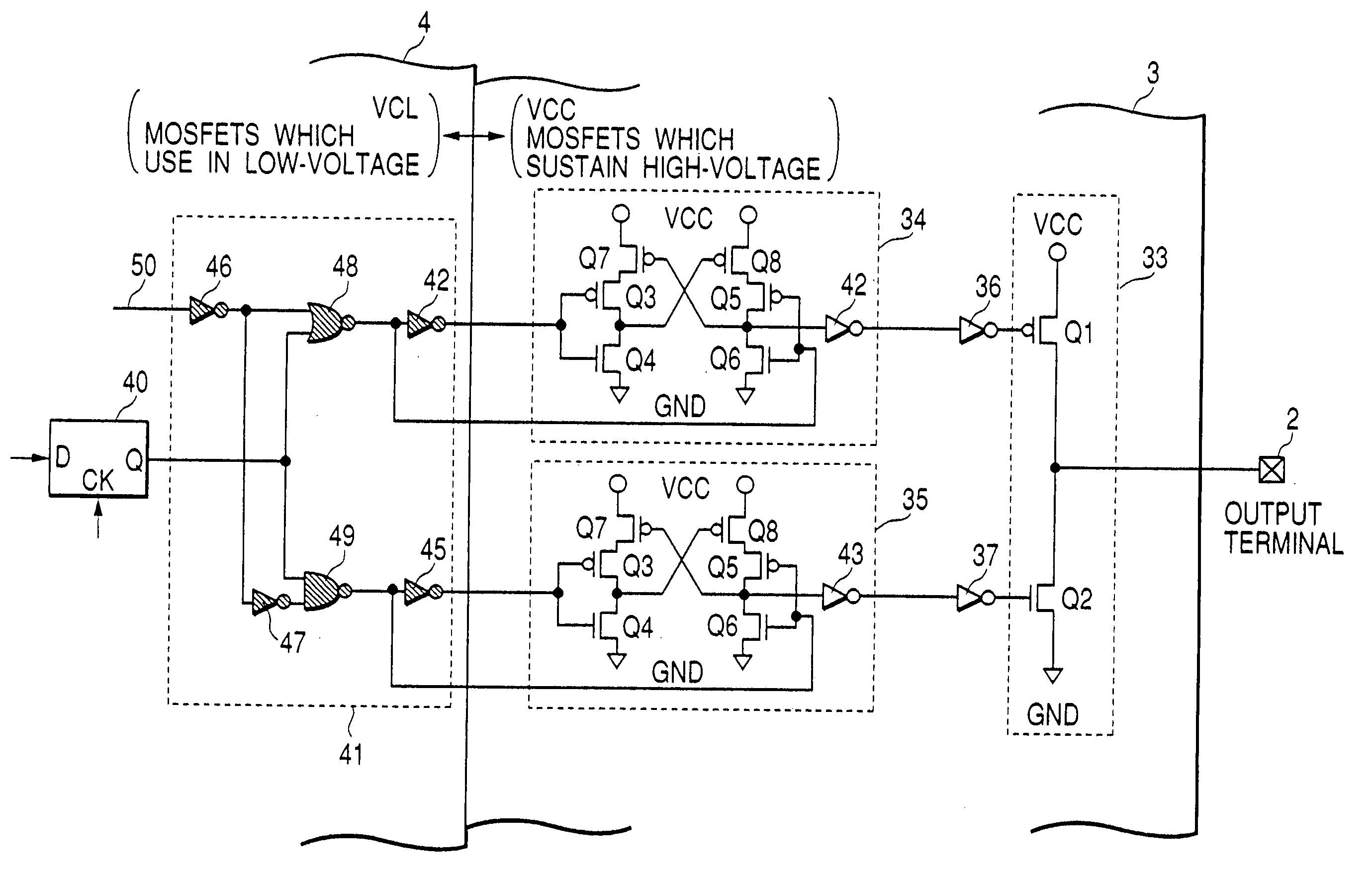
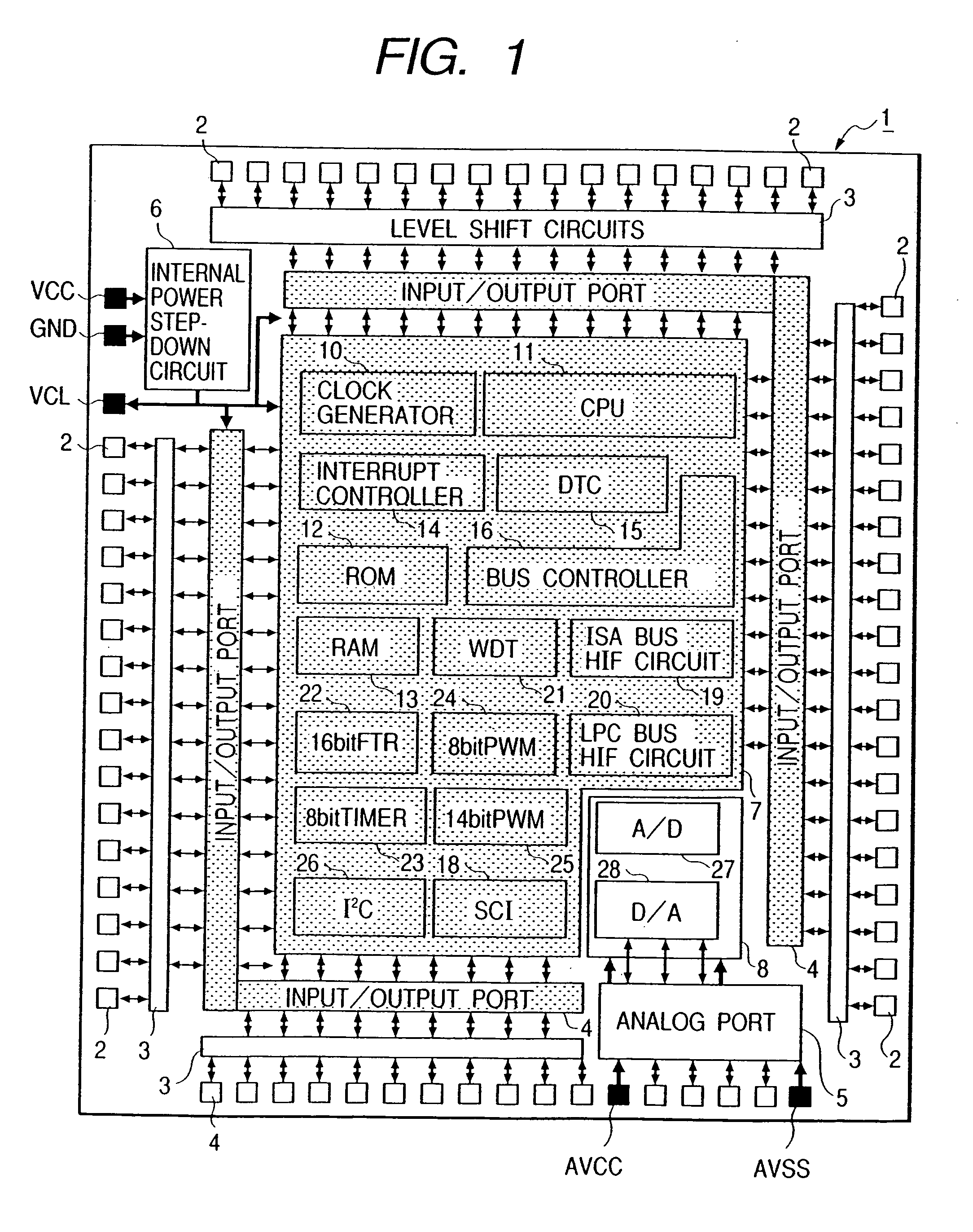
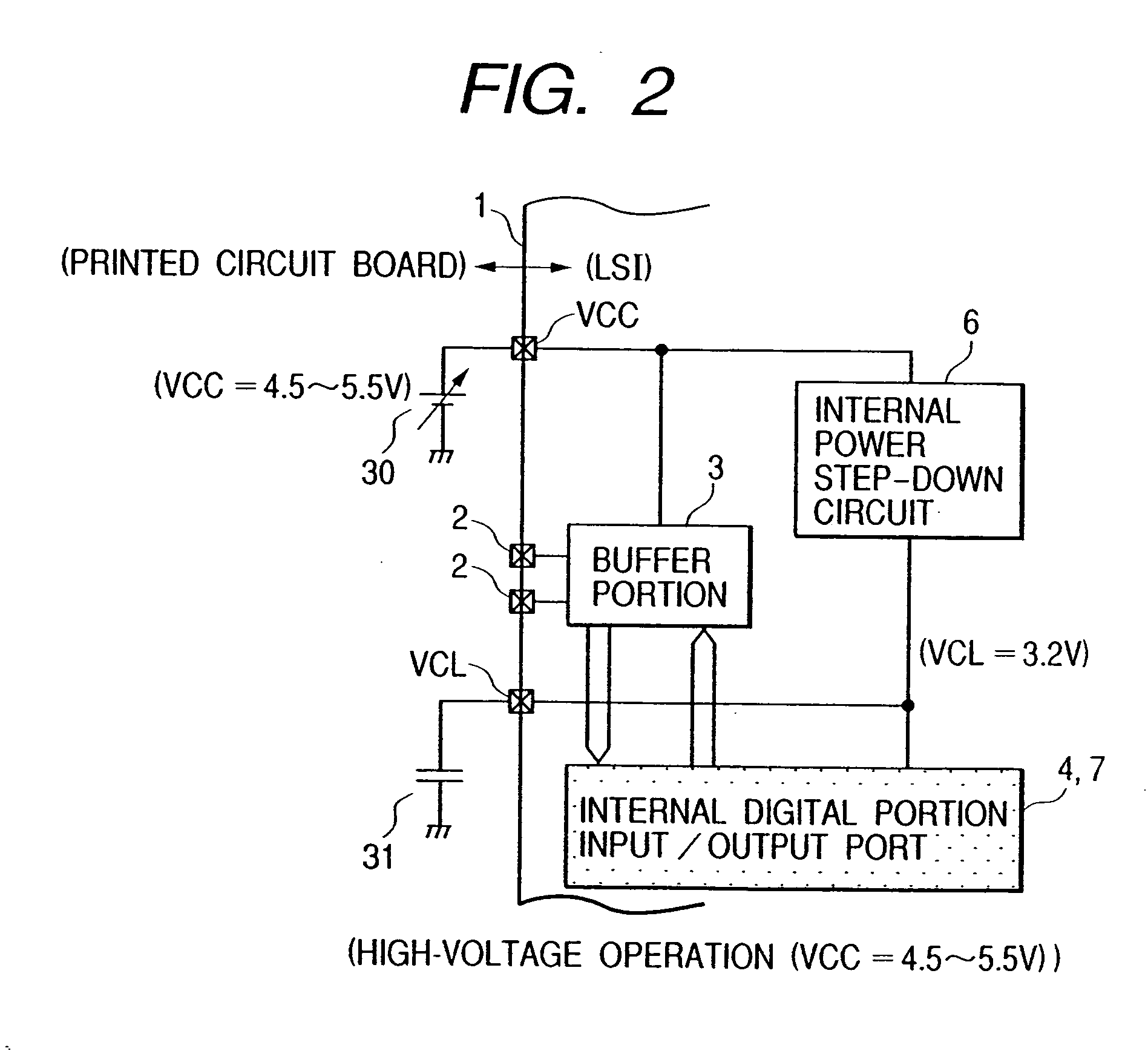
[0049]FIG. 1 shows a microcomputer as an example of a semiconductor integrated circuit according to the invention. A microcomputer 1 shown in the diagram is formed on a semiconductor substrate (chip) made of single crystal silicon or the like by, for example, a known CMOS integrated circuit fabricating technique. Although not limited, a number of output terminals 2 such as bonding pads are disposed around the chip. On the inside of the output terminals 2, a buffer portion 3, an input / output port 4, an analog port 5, and an internal power step-down circuit 6 are disposed. In the center portion, an internal digital portion 7 and an analog portion 8 are disposed.

[0050] The input / output port 4 and the internal digital portion 7 form a first circuit constructed by a MOS transistor having a relatively low breakdown voltage, and the like. On the other hand, the buffer portion 3 forms a second circuit of a high breakdown voltage, which is constructed by a MOS transistor having a relatively...


PUM


Abstract

A semiconductor integrated circuit includes a first circuit and a second circuit having a breakdown voltage higher than that of the first circuit. Operation voltages of the first and second circuits can be made equal to or different from each other. The second circuit has a level shift circuit for shifting the level of an output signal of the first circuit in accordance with an operation voltage of the second circuit, an external output buffer having an input that can receive, selectively, an output signal of the level shift circuit or an input signal that bypasses the level shift circuit. When the first and second circuits operate with a low voltage, bypass is selected. In high-voltage operation and burn-in, the level shift circuit is selected.

Description

BACKGROUND OF THE INVENTION [0001] The present invention relates to a semiconductor integrated circuit technique for addressing increase in speed of external output operation synchronized with a clock signal. More particularly, the invention relates to, for example, a semiconductor integrated circuit using, in an external interface portion, a MOS transistor having a breakdown voltage higher than that of an internal circuit and, further, to a technique effective to be applied to a burn-in method of such a semiconductor integrated circuit. [0002] Japanese Unexamined Patent Application No. 9(1996)-8632 discloses a technique of stepping down an external power supply voltage within an LSI and making an external interface circuit operate with an external power supply voltage by using the stepped-down voltage as an operation power source of an internal circuit from a viewpoint of reduction in the size of a circuit device, reduction in power consumption, and the like. Japanese Unexamined Pa...

Claims


Application Information

Patent Timeline
Patent Type & Authority Applications(United States)
IPC IPC(8): G01R31/30G01R31/28G01R31/316H01L21/822H01L27/04H03K19/0175H03K19/0185H03L5/00
CPCH03K19/018585H03K19/01855
Inventor TAHARA, SHIGEMITSUKATAGIRI, DAISUKESHIMANUKI, TAKESHIOSHIBA, MASASHI
Owner RENESAS ELECTRONICS CORP
Why Eureka
Try Eureka