Laminate body, method, and apparatus for manufacturing ultrathin substrate using the laminate body

a technology of laminate body and ultrathin substrate, which is applied in the direction of diffusion transfer process, photosensitive materials, instruments, etc., can solve the problems that the method cannot be practically used as a method of thinning a semiconductor wafer, and the method has not yet achieved a remarkable improvement over the present level of wafer thickness, etc., and achieves the effect of easy peeling

Active Publication Date: 2005-10-20
3M INNOVATIVE PROPERTIES CO
View PDF14 Cites 139 Cited by
  • Summary
  • Abstract
  • Description
  • Claims
  • Application Information

AI Technical Summary

Benefits of technology

[0004] Accordingly, the object of the present invention is to provide a laminated body in which a substrate to be ground is fixed on a support and the substrate to be ground can be easily peeled off from the support. The object of the present invention includes providing a method for manufacturing the laminated body, and a method and an apparatus for manufacturing an ultrathin substrate using the laminated body.

Problems solved by technology

Usually, in conventional techniques of grinding the back side, or surface, of a wafer and conveying it while holding the wafer with only a backgrinding protective tape, thickness reduction can be accomplished in practice only to a thickness of about 150 micrometers (μm) because of problems such as uneven thickness of the ground wafer or warping of the wafer with protective tape after grinding.
However, this method has not yet attained a remarkable improvement over the present level of wafer thickness which may be obtained without encountering the aforementioned problems of unevenness or warpage.
According to this method, a wafer can be processed to a lower thickness level as compared with the above-described method, however, the ultrathin wafer cannot be separated from the support without breaking the wafer and therefore, this method cannot be practically used as a method of thinning a semiconductor wafer.

Method used


Image

  • Laminate body, method, and apparatus for manufacturing ultrathin substrate using the laminate body
  • Laminate body, method, and apparatus for manufacturing ultrathin substrate using the laminate body
  • Laminate body, method, and apparatus for manufacturing ultrathin substrate using the laminate body

Examples


example 1

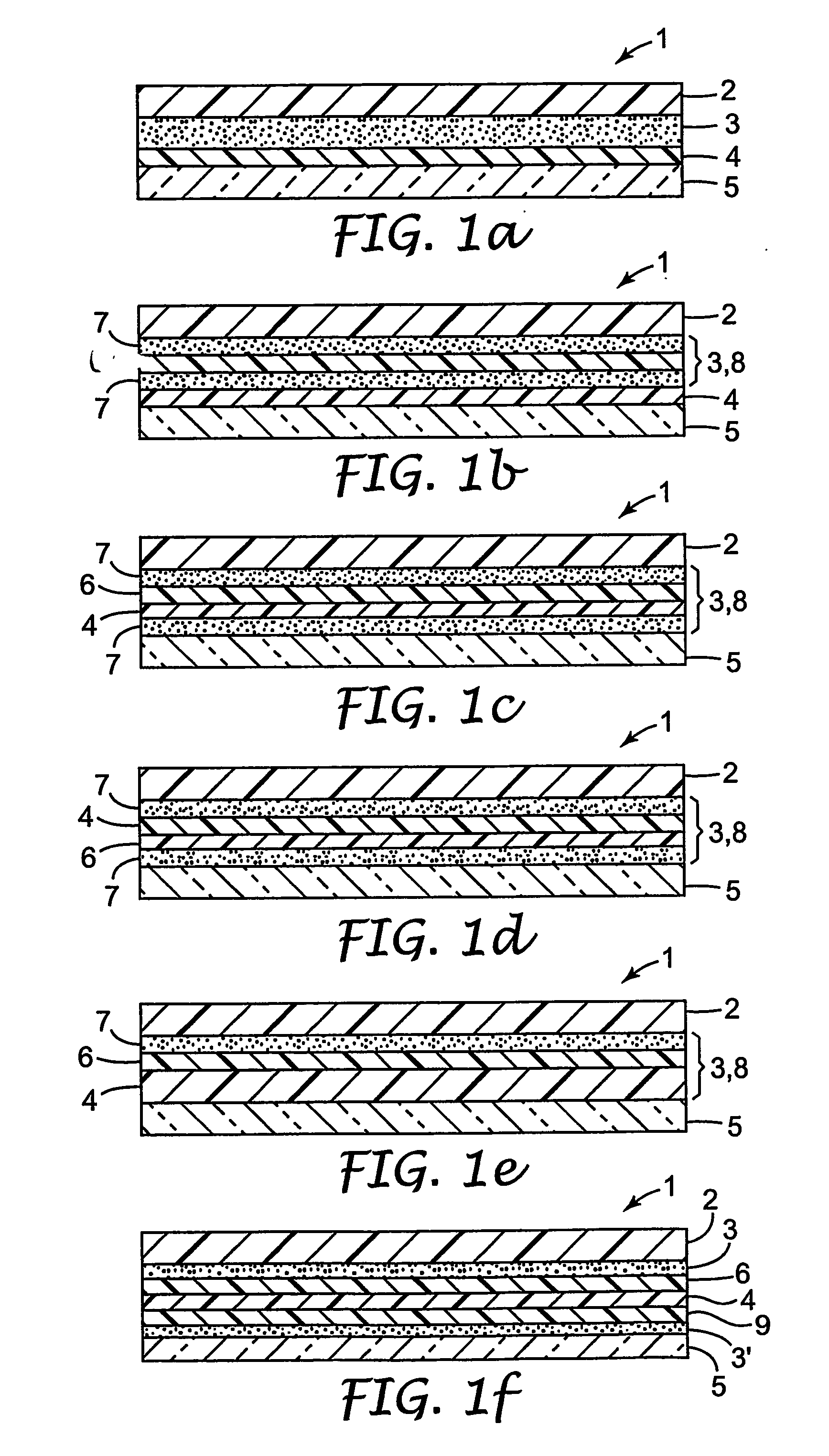
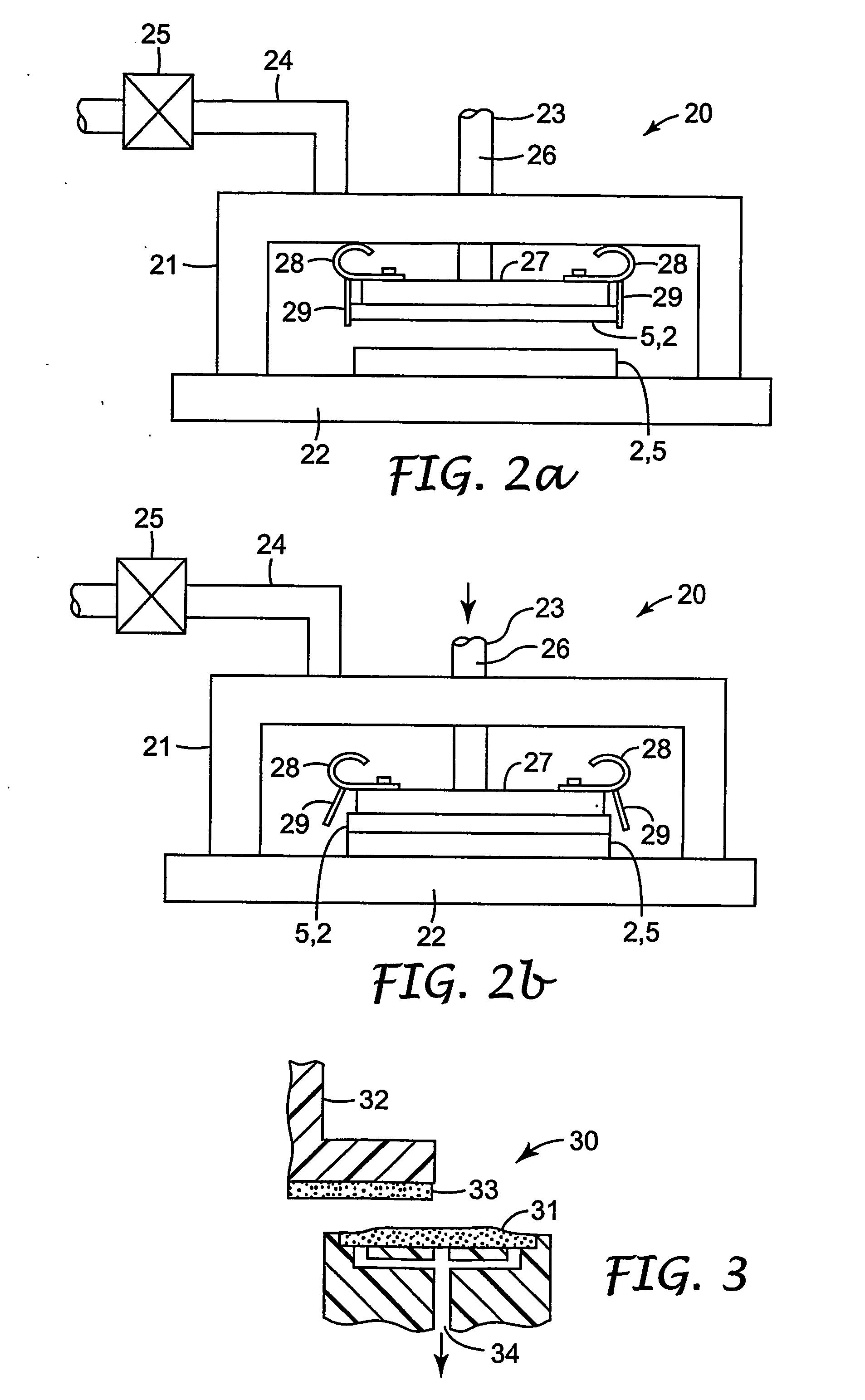
[0085] A glass substrate of 220 mm (diameter)×1.0 mm (thickness) was used as the light permeable support, and a silicon wafer of 200 mm (diameter)×750 μm (thickness) was used as the wafer. A 10% solution (in propylene glycol methylether acetate solvent) of a photothermal conversion layer precursor having the composition shown in Table 1 above was coated on the glass substrate by spin coating. This was dried by heating and then cured by ultraviolet (UV) irradiation to form a photothermal conversion layer on the support. A joining layer precursor having the composition shown in Table 2 above was coated on the wafer similarly by spin coating. The glass substrate and the wafer were laminated to each other in a vacuum adhesion device as shown in FIG. 2 and thereon, was irradiated with UV light to cure the joining layer precursor, thereby obtaining a laminated body. This laminated body had a configuration of glass substrate / photothermal conversion layer / joining layer / silicon wafer, the th...

example 2

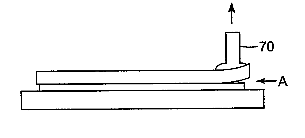
[0089] In this Example, the test was performed in the same manner as in Example 1 except for the following modifications. As the photothermal conversion layer precursor, a 20% solution (in propylene glycol methylether acetate) having the composition at a solid content ratio shown in Table 3 below was used. Furthermore, in order to prevent re-adhesion due to the weight of the glass substrate during laser irradiation, an L-shaped hook was inserted into the edge part of the glass substrate and hung up with a spring, whereby re-adhesion due to the weight of the glass substrate during laser beam irradiation was prevented. Similarly to Example 1, a silicon wafer having a thickness of 50 μm could be obtained without damaging the wafer.

TABLE 3Photothermal Conversion LayerSolid Content RatioRaven 76027.64%Disperbyk 16113.82%Ebecryl 880450.49%Irgacure 369 7.00%Irgacure 184 1.05%Total100.00% 

Raven 760 (Columbian Carbon Japan Ltd.): carbon black; Disperbyk 161 (BYK Chemie): dispersant (30% in...

example 3

[0090] In this Example, the test was performed in the same manner as in Example 2 except that a 10% solution (in propylene glycol methylether acetate) having the composition at a solid content ratio shown in Table 4 below was used as the photothermal conversion layer precursor. This photothermal conversion layer precursor is a polymer solution containing carbon black and therefore, the photothermal conversion layer was formed only by drying.

TABLE 4Photothermal Conversion LayerSolid Content RatioRaven 76030.06%Disperbyk 16115.03%UR830054.91%Total100.00% 

Raven 760 carbon black; Disperbyk 161 dispersant; UR8300 polyurethane polyester.

[0091] A silicon wafer having a thickness of 50 μm could be obtained without damaging the wafer by the same operation similarly to Example 1.


PUM

PropertyMeasurementUnit
transparentaaaaaaaaaa
thicknessaaaaaaaaaa
thicknessaaaaaaaaaa

Abstract

Provided is a laminated body (1) comprising a substrate (2) to be ground and a support (5), where the substrate (2) is ground to a very small thickness and can then be separated from the support (5) without damaging the substrate (2). One embodiment of the present invention is a laminated body (1) comprising a substrate (2) to be ground, a joining layer (3) in contact with the substrate (2) to be ground, a photothermal conversion layer (4) comprising a light absorbing agent and a heat decomposable resin, and a light transmitting support (5). After grinding the substrate surface which is opposite that in contact with the joining layer (3), the laminated body (1) is irradiated through the light transmitting support (5) and the photothermal conversion layer (4) decomposes to separate the substrate (2) and the light transmitting support (5).

Description

TECHNICAL FIELD [0001] The present invention relates to a laminated body where a substrate to be ground, such as silicon wafer, fixed on a support can be easily separated from the support, and also relates to a method and an apparatus for manufacturing this laminated body and a method and an apparatus for producing a thinned substrate. BACKGROUND [0002] In various fields, reducing the thickness of a substrate often is desired. For example, in the field of quartz devices, reducing the thickness of a quartz wafer is desired so as to increase the oscillation frequency. Particularly, in the semiconductor industry, efforts to further reduce the thickness of a semiconductor wafer are in progress to respond to the goal of reducing the thickness of semiconductor packages as well as the high-density fabrication by chip lamination technology. Thickness reduction is performed by so-called back side grinding of a semiconductor wafer on the surface opposite that containing pattern-formed circuit...

Claims


Application Information

Patent Timeline
Patent Type & Authority Applications(United States)
IPC IPC(8): B32B43/00H01L21/00H01L21/304H01L21/68
CPCB32B43/006H01L21/67132H01L21/6835H01L2221/6839H01L2221/68318H01L2221/68327H01L21/6836
Inventor NODA, KAZUKIIWASAWA, MASARU
Owner 3M INNOVATIVE PROPERTIES CO
Why Eureka
Try Eureka