Piezoelectric device comprising ultrahighly-orientated aluminum nitride thin film and its manufacturing method

a technology of aluminum nitride and thin film, which is applied in the direction of device material selection, semiconductor/solid-state device details, vacuum evaporation coating, etc., can solve the problems of insufficient piezoelectricity, no electrode can be provided between the substrate and the the nitride film has great rocking curve full width half maximum,

Inactive Publication Date: 2005-10-27
NAT INST OF ADVANCED IND SCI & TECH
View PDF4 Cites 31 Cited by
  • Summary
  • Abstract
  • Description
  • Claims
  • Application Information

AI Technical Summary

Benefits of technology

[0014] A method of manufacturing a piezoelectric element using a superhigh-oriented aluminum nitride thin film in accordance with the present invention is characterized by including the sequential steps of: forming a bottom electrode on a substrate from such an oriented W layer that a (111) plane of W is parallel to a surface of the substrate by sputtering at a temperature from room temperature to a low temperature at which no spaces develop between W particles; and forming a piezoelectric body thin film of a c-axis-oriented aluminum nitride thin film having a RCFWHM not exceeding 2.5° on the bottom electrode; and forming a top electrode on the piezoelectric body thin film.
[0015] Another method of manufacturing a piezoelectric element using a superhigh-oriented aluminum nitride thin film in accordance with the present invention is characterized by including the sequential steps of: in forming, on a substrate, a bottom electrode of a two- or more-layered stack structure including an adhesive layer adhering to the substrate, firstly depositing the adhesive layer by sputtering at a temperature from room temperature to a low temperature at which no spaces develop between particles and then depositing as a surface layer of the bottom electrode a metal layer by sputtering at a temperature from room temperature to a low temperature at which no spaces develop between particles so that the metal layer exhibits such orientation that a crystal plane of a metal is parallel to a surface of the substrate, by using such a metal having an electronegativity of around 1.4 that a crystal plane of the metal has an identical atomic configuration to an atomic configuration on a (001) plane of aluminum nitride and an almost equal atomic distance to an atomic distance on the (001) plane; forming a piezoelectric body thin film of a c-axis-oriented aluminum nitride thin film having a RCFWHM not exceeding 2.5° on the bottom electrode; and forming a top electrode on the piezoelectric body thin film.
[0016] Another method of manufacturing a piezoelectric element using a superhigh-oriented aluminum nitride thin film in accordance with the present invention is characterized by including the sequential steps of: in forming, on a substrate, a bottom electrode of a two- or more-layered stack structure including an adhesive layer adhering to the substrate, firstly depositing the adhesive layer by sputtering at a temperature from room temperature to a low temperature at which no spaces develop between particles and then depositing as a surface layer an oriented W, Pt, Au, or Ag layer that a (111) plane of W, Pt, Au, or Ag is parallel to a surface of the substrate by sputtering at a temperature from room temperature to a low temperature at which no spaces develop between particles; forming a piezoelectric body thin film of a c-axis-oriented aluminum nitride thin film having a RCFWHM not exceeding 2.5° on the bottom electrode; and forming a top electrode on the piezoelectric body thin film.

Problems solved by technology

These aluminum nitride films however have great rocking curve full width half maximums (RCFWHMs) of about 3.0° or more, a measure of c-axis orientation, and insufficient piezoelectricity.
Therefore, no electrode can be provided between the substrate and the aluminum nitride thin film, which renders it difficult to use the film as an piezoelectric element.
When fabricated on an electrode, the film may create cracks in the electrodes or peel off the substrate together with the electrodes, raising serious problems in the applying to piezoelectric elements.

Method used


Image

  • Piezoelectric device comprising ultrahighly-orientated aluminum nitride thin film and its manufacturing method
  • Piezoelectric device comprising ultrahighly-orientated aluminum nitride thin film and its manufacturing method
  • Piezoelectric device comprising ultrahighly-orientated aluminum nitride thin film and its manufacturing method

Examples


example 1

Effects of Bottom Electrode

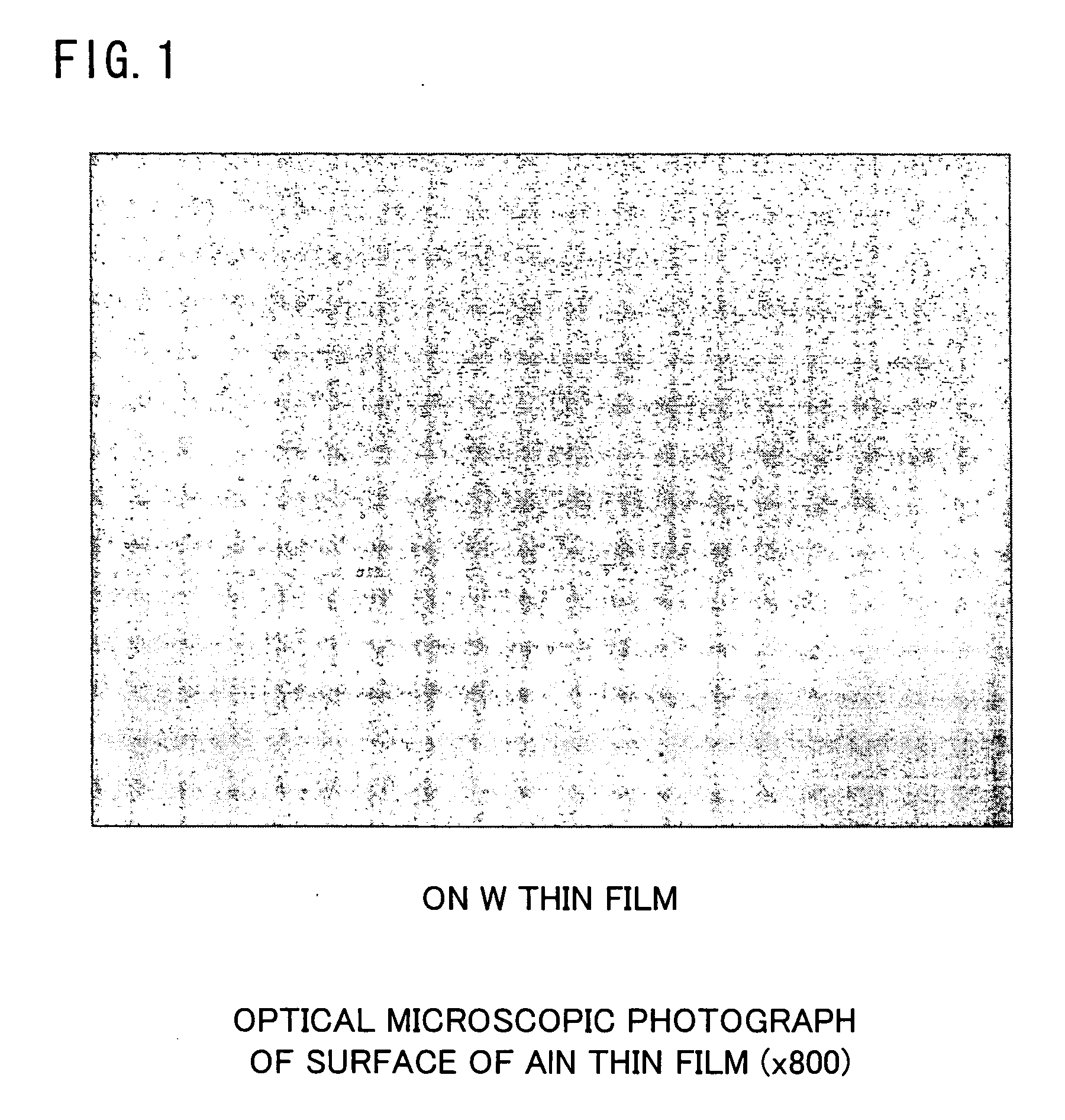
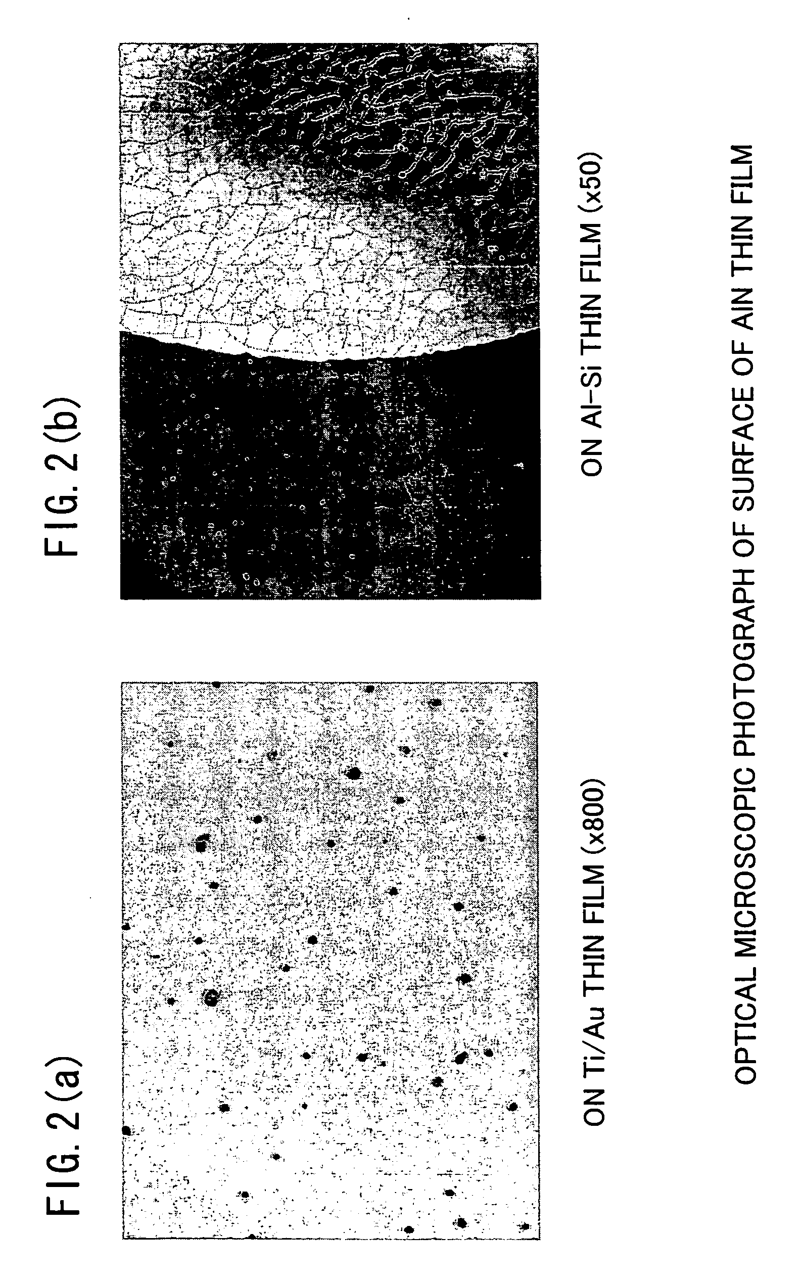
[0056] Most researches into AlN thin film growth on a conductor have been conducted around the improvement of iron's corrosion resistance and the growth on Al electrodes for use in a surface acoustic wave (SAW) filter. Only a small number of researches have been conducted into the growth on other conductors. According to reports, the highest orientation AlN thin film so far is fabricated on an Au thin film on a glass substrate and exhibits a rocking curve full width half maximum of 3°. Accordingly, to find the high orientation AlN thin film on a bottom electrode, an AlN thin film was fabricated on 20 types of conductor thin films, to observe the effects of a crystal structure to the AlN thin film. Most of the 20 types of conductor thin films were processed by sputtering at room temperature. Table 1 shows XRD measurements on the obtained AlN thin films. The substrates were all made of glass.

[0057] Specifically, each bottom electrode specimen was deposited...

example 2

Effects of Stacked Bottom Electrode

[0063] There has been no single report on stack effects of a bottom electrode for the AlN thin film. Accordingly, we examined effects on the AlN thin film crystal structure, such as orientation and crystallinity, of two and three metal thin films being stacked together.

[0064] We examined bottom electrodes containing Pt, i.e. Ti / Pt and Cr / Pt, which had high orientation and high crystallinity. The substrate was a quartz glass (20 mm×20 mm×1.1 mm). The deposition conditions for the bottom electrode were a pressure of 1.0×10⁻¹ Pa, a nitrogen gas partial pressure ratio of 0%, no substrate heating, and a target introduction electric power of 200 W. The film thickness was varied depending on the material. In addition, the deposition conditions for the aluminum nitride were a pressure of 1.3×10⁻¹ Pa, a nitrogen gas partial pressure ratio of 60%, a substrate temperature of 300° C., and a target introduction electric power of 200 W. The film thickness was ...

example 3

Effects of Fabrication Temperature of Bottom Electrode

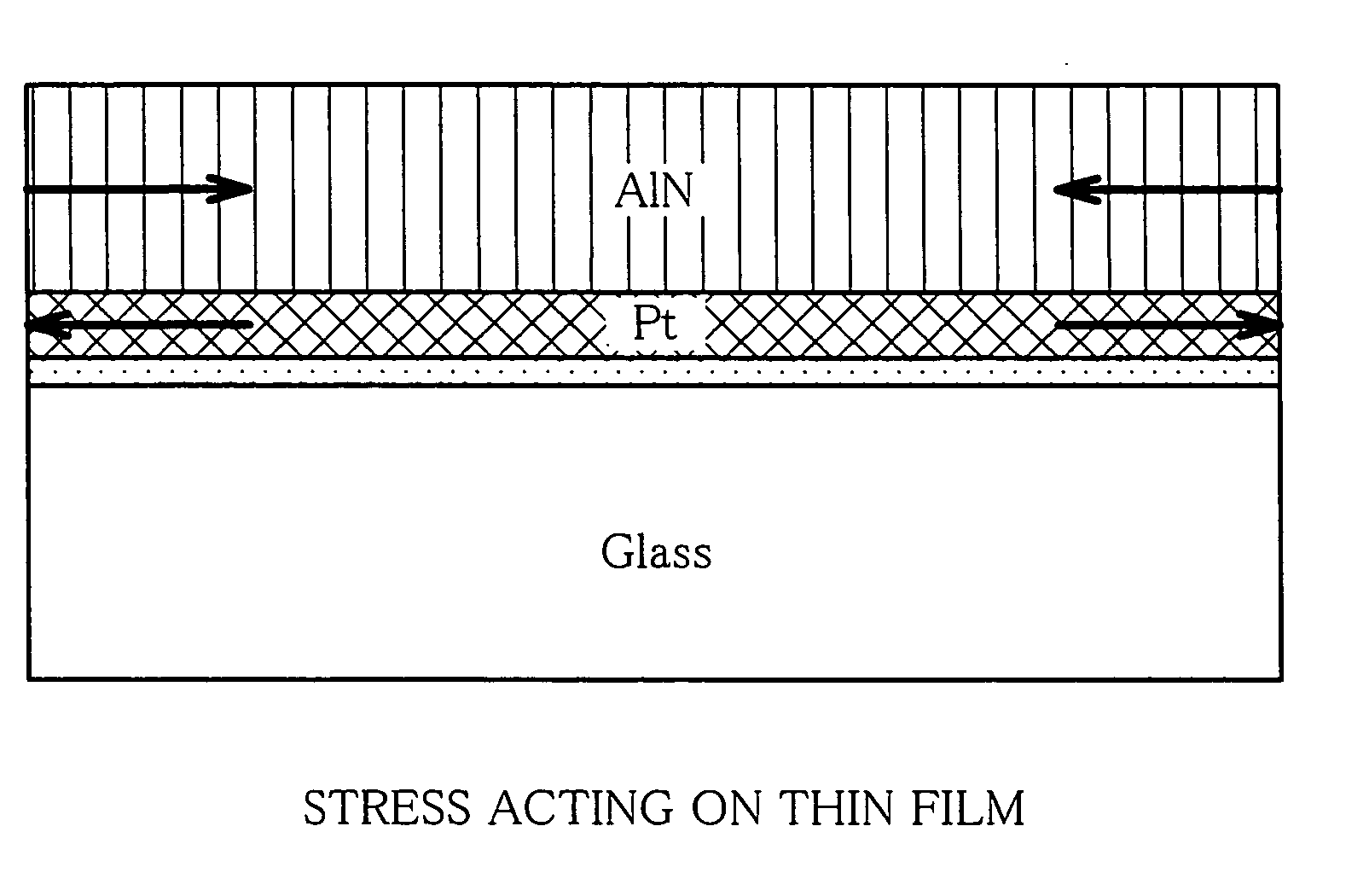
[0077] Possible causes of cracks and peeling are differing thermal expansion coefficients of the substrate and bottom electrode and the AlN. Accordingly, to reduce the effects of the differing thermal expansion coefficients for prevention of cracks and peeling, the effects of the fabrication temperature of the bottom electrode was examined. Ti / Pt thin films with high orientation were used as bottom electrodes. Ti / Pt bottom electrodes were fabricated at room temperature, 300° C., and about 400° C. The top electrode was an Al thin film fabricated by vacuum vapor deposition. Three samples were simultaneously fabricated at different temperatures, to examine short-circuiting of the samples.

[0078] When the bottom electrode was fabricated at room temperature, all the samples experienced no short circuiting. In contrast, when the bottom electrode was fabricated at 300° C., one third of the samples experienced no short circuiting. When ...


PUM

PropertyMeasurementUnit
temperatureaaaaaaaaaa
thicknessaaaaaaaaaa

Abstract

The present invention has an objective to provide a high performance piezoelectric element in which is formed an aluminum nitride thin film free from hillocks, cracks, and peeling which exhibits superhigh c-axis orientation, by forming a bottom electrode from a W layer with no intervening adhesive layer on a glass or other cheap substrate. The piezoelectric element of the present invention is a piezoelectric element using a superhigh-oriented aluminum nitride thin film characterized in that the piezoelectric element is free from hillocks, cracks, and peeling and includes a stack structure in which a bottom electrode, a piezoelectric body thin film, and a top electrode are sequentially formed on a substrate; the bottom electrode is made of an oriented W layer of which a (111) plane of W is parallel to a surface of the substrate; and the piezoelectric body thin film is formed of a c-axis-oriented aluminum nitride thin film having a rocking curve full width half maximum (RCFWHM) not exceeding 2.5°.

Description

TECHNICAL FIELD [0001] The present invention relates to piezoelectric elements using a thin film, provided on a glass or other cheap substrate, in which aluminum nitride has a high c-axis orientation and manufacturing methods of such elements. BACKGROUND ART [0002] Aluminum nitride is a promising material in efforts to making more compact, thinner piezoelectric elements for, among other factors, its high fabricability into thin film. However, to utilize aluminum nitride as an piezoelectric element, the aluminum nitride needs to be oriented only along the c-axis. The more c-axis-oriented, the more piezoelectric. In addition, to use an aluminum nitride thin film as a piezoelectric element, the film needs be flanked on top and bottom by electrodes. [0003] Thin films of c-axis-oriented aluminum nitride have been reportedly produced on glass and other substrates by various methods (T. Shiosaki, T. Yamamoto, T. Oda, A. Kawabata, Appl. Phys. Lett., 36 (1980) 643). There are also reports ab...

Claims


Application Information

Patent Timeline
Patent Type & Authority Applications(United States)
IPC IPC(8): H01L41/09H01L41/18C23C14/34H01L41/22H01L41/29H01L41/316
CPCY10T29/42H01L41/316H10N30/076
Inventor AKIYAMA, MORITOUENO, NAOHIROTATEYAMA, HIROSHISUNAGAWA, YOSHITAKAUMEUCHI, YOSHIHIROJINUSHI, KEIICHIRO
Owner NAT INST OF ADVANCED IND SCI & TECH
Why Eureka
Try Eureka