Integrated circuit package with different hardness bump pad and bump and manufacturing method therefor

a technology of integrated circuits and bumps, which is applied in the direction of semiconductor devices, semiconductor/solid-state device details, electrical apparatus, etc., can solve the problems of limited current technology, high corrosion resistance of aluminum and aluminum alloys, and long elude the ability of those skilled in the art to solve the problem, etc., to reduce the size of the technology and reduce the resistance

Inactive Publication Date: 2005-11-03
STATS CHIPPAC LTD
View PDF7 Cites 26 Cited by
  • Summary
  • Abstract
  • Description
  • Claims
  • Application Information

AI Technical Summary

Benefits of technology

[0011] The TAB using the bump technology of the present invention provides bonds that hold a

Problems solved by technology

Aluminum and aluminum alloys are highly susceptible to corrosion if left exposed to the environment and, as a result, one or two protective passivation layers of silicon oxide, silicon nitride or polyimide are applied.
But more products now require passivation laye

Method used


Image

  • Integrated circuit package with different hardness bump pad and bump and manufacturing method therefor
  • Integrated circuit package with different hardness bump pad and bump and manufacturing method therefor
  • Integrated circuit package with different hardness bump pad and bump and manufacturing method therefor

Examples


Embodiment Construction

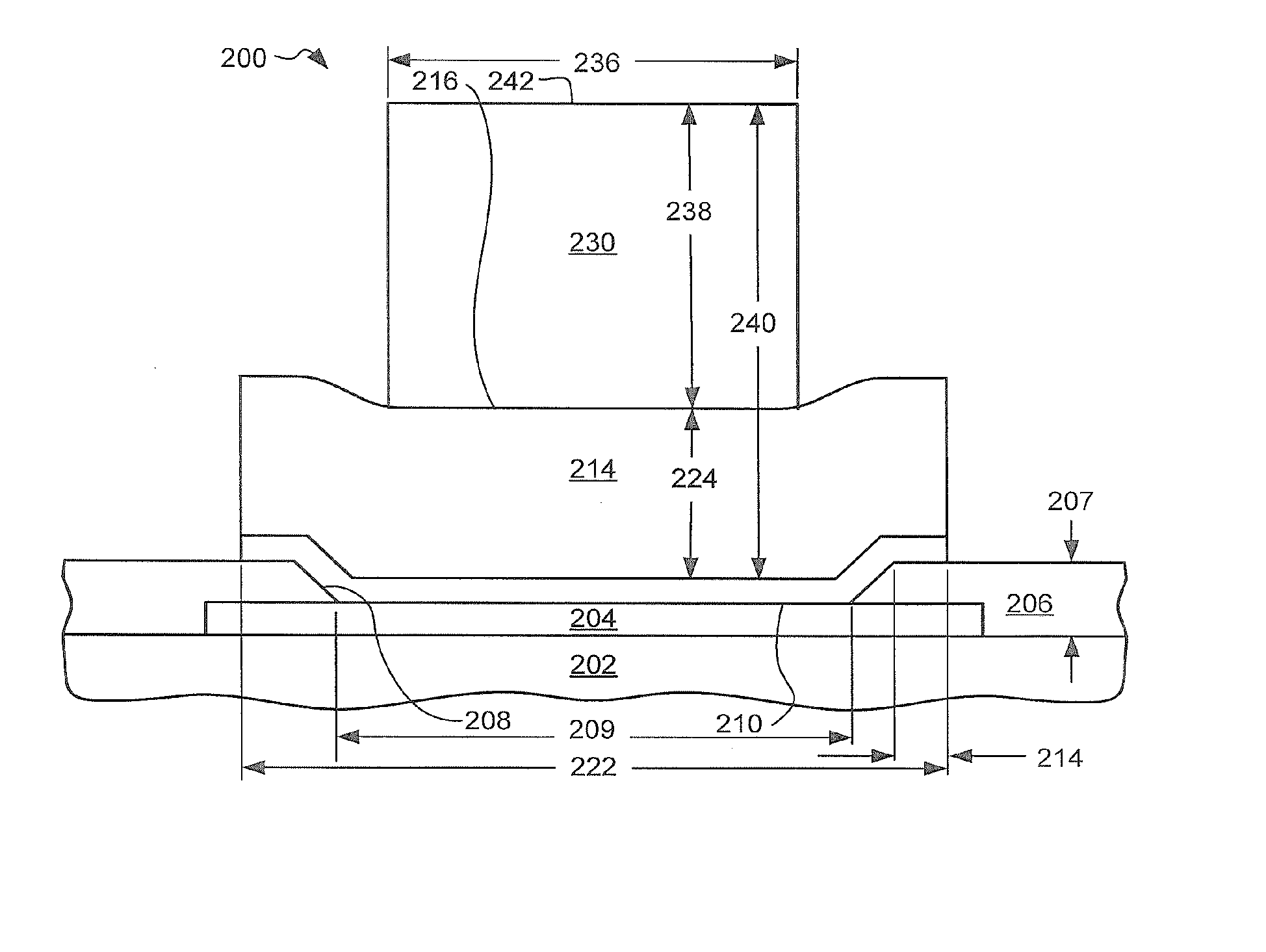
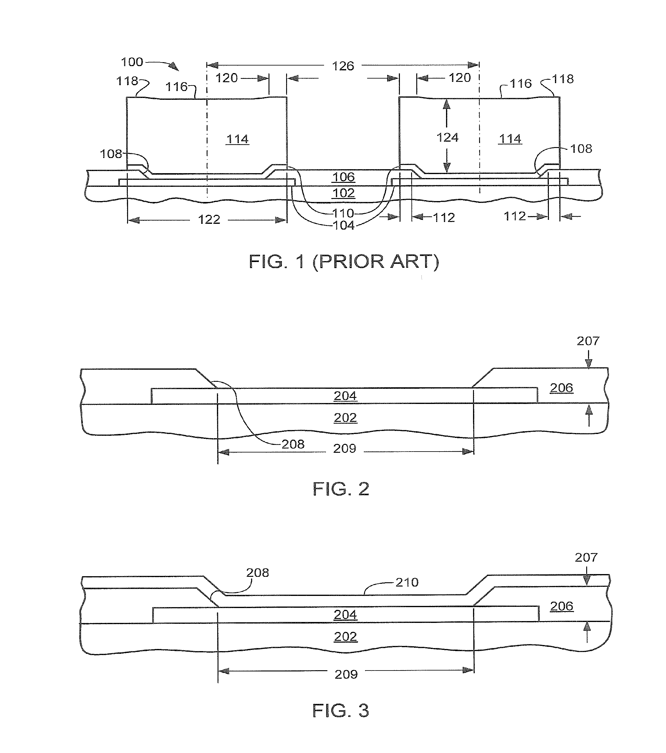
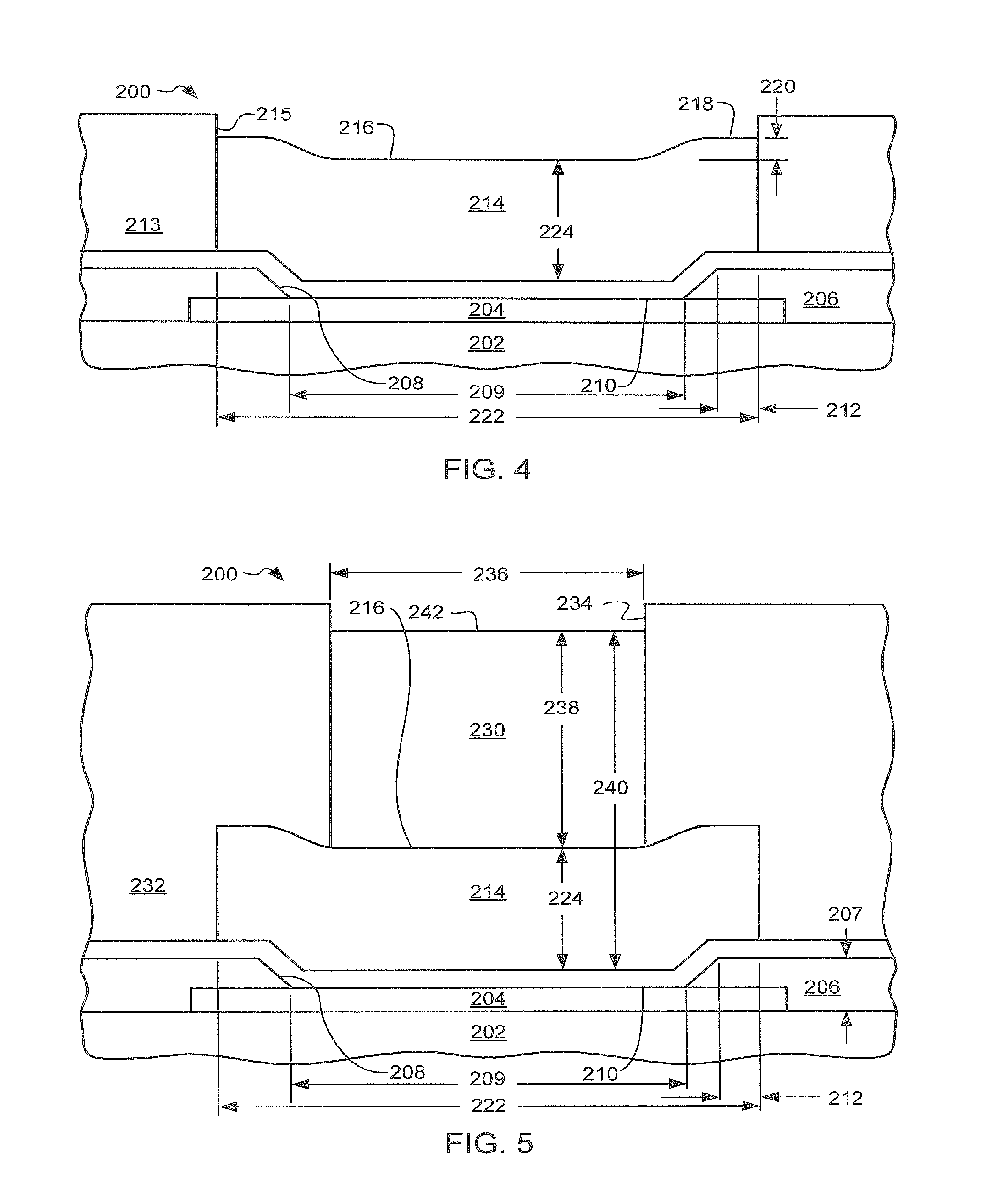
[0020] Referring now to FIG. 1 (PRIOR ART), therein is shown a cross-sectional view of a integrated circuit package 100 in the prior art. The integrated circuit package 100 includes an integrated circuit 102 having input / output contact pads 104 under a passivation layer 106.

[0021] The term “horizontal” as used in herein is defined as a plane parallel to the conventional plane or under surface of the integrated circuit package, such as the integrated circuit package 100, regardless of its orientation. The term “vertical” refers to a direction perpendicular to the horizontal as just defined. Terms, such as “on”, “above”, “below”, “side”, “higher”, “lower”, “over”, and “under”, are defined with respect to the horizontal plane. The term “processing” as used herein includes deposition of material or photoresist, patterning, exposure, development, etching, cleaning, and / or removal of the material or photoresist as required in forming a described structure.

[0022] The passivation layer 10...


PUM


Abstract

A manufacturing method for an integrated circuit package is provided including forming a contact pad under a passivation layer on an integrated circuit, forming an opening in the passivation layer exposing the contact pad, and forming an under bump metallurgy over the contact pad and the passivation layer. The method further includes forming a bump pad over the under bump metallurgy of a material having a first hardness and forming a bump on and over the bump pad, the bump having a top flat surface and of a material having a second hardness softer than the first hardness.

Description

CROSS-REFERENCE TO RELATED APPLICATION(S) [0001] This is a continuation-in-part of co-pending U.S. patent application Ser. No. 10 / 251,512 filed Sep. 19, 2002.TECHNICAL FIELD [0002] The present invention relates generally to the fabrication of semiconductor integrated circuit packages, and more specifically to packages with metal bumps for making electrical connections. BACKGROUND ART [0003] Electronic products have become an aspect of every day life from televisions to cell phones to wristwatches. The hearts of these electronic products are integrated circuits, which continue to be made smaller and more reliable while increasing performance and speed. [0004] An integrated circuit is typically packaged in a tiny box-type structure usually on the order of a few millimeters per side. The integrated circuit package generally has cylindrical terminals formed through a passivation layer of the integrated circuit near its edges for directly bonding the integrated circuit package to a foil-...

Claims


Application Information

Patent Timeline
IPC IPC(8): H01L21/60H01L23/485
CPCH01L24/11H01L2224/1147H01L2924/0001H01L2224/13144H01L2924/01033H01L2224/13099H01L2924/01013H01L2924/01022H01L2924/01027H01L2924/01029H01L2924/01074H01L2924/01078H01L2924/01079H01L2924/01082H01L2924/14H01L24/13H01L2924/00014H01L2224/05027H01L2224/05022H01L2224/05001H01L2224/05572H01L2224/05124H01L2224/05644H01L2224/0347H01L24/03H01L24/05H01L2224/0346H01L2224/05166H01L2224/05582H01L2224/1146H01L2224/03914H01L2224/11906
Inventor JIN, YONGGANG
Owner STATS CHIPPAC LTD
Why Eureka
Try Eureka