Printer using direct-coupled emissive array

a printing device and photoemissive array technology, applied in printing, electrical equipment, semiconductor devices, etc., can solve the problems of limited resolution, large volume of crt imaging devices, limited resolution, etc., and achieve high light efficiency, good sharpness and contrast

Inactive Publication Date: 2005-11-03
EASTMAN KODAK CO
View PDF14 Cites 8 Cited by
  • Summary
  • Abstract
  • Description
  • Claims
  • Application Information

AI Technical Summary

Benefits of technology

[0016] It is an advantage of the present invention that it provides a compact and potentially low-cost component arrangement for printing using a direct-coupled emissive array. The printing apparatus of the present invention uses a minimum number of components, not requiring optical components except those integrated into the direct-coupled emissive array, and provides the advantages of the contact printing model described in the background section above. The printing apparatus of the present invention

Problems solved by technology

While varying degrees of success have been achieved in deploying each of these technologies, some drawbacks remain.
CRT imaging devices, for example, are bulky, limited in resolution, and relatively expensive.
Laser scanning devices are characterized by relatively high cost and substantial optical and mechanical complexity.
DMD printers also require costly support optics and are limited in the available resolution.
Supporting optics for digital printing systems employing CRT, scanned laser, LCD, and DMD imaging devices add cost, size, and complexity to printing apparatus design.
However, they still require separate projection optics for image forming on photosensitive media.
The need for projection optics still poses limitations to the use of OLED devices in building very compact printer systems.
Without the use of interposed optics for imaging, contact printing has the advantage of allowing the implementation of potentially compact printer systems, but is not suitable for many digital printing technologies.
In particular, light path constraints prevent laser-, LCD- and DMD-based imaging systems from being used in contact printing configuration.
Thus, although the apparatus of U.S. Pat. No. 4,484,233 does not require lens components for exposure of the photosensitiv

Method used


Image

  • Printer using direct-coupled emissive array
  • Printer using direct-coupled emissive array
  • Printer using direct-coupled emissive array

Examples


Embodiment Construction

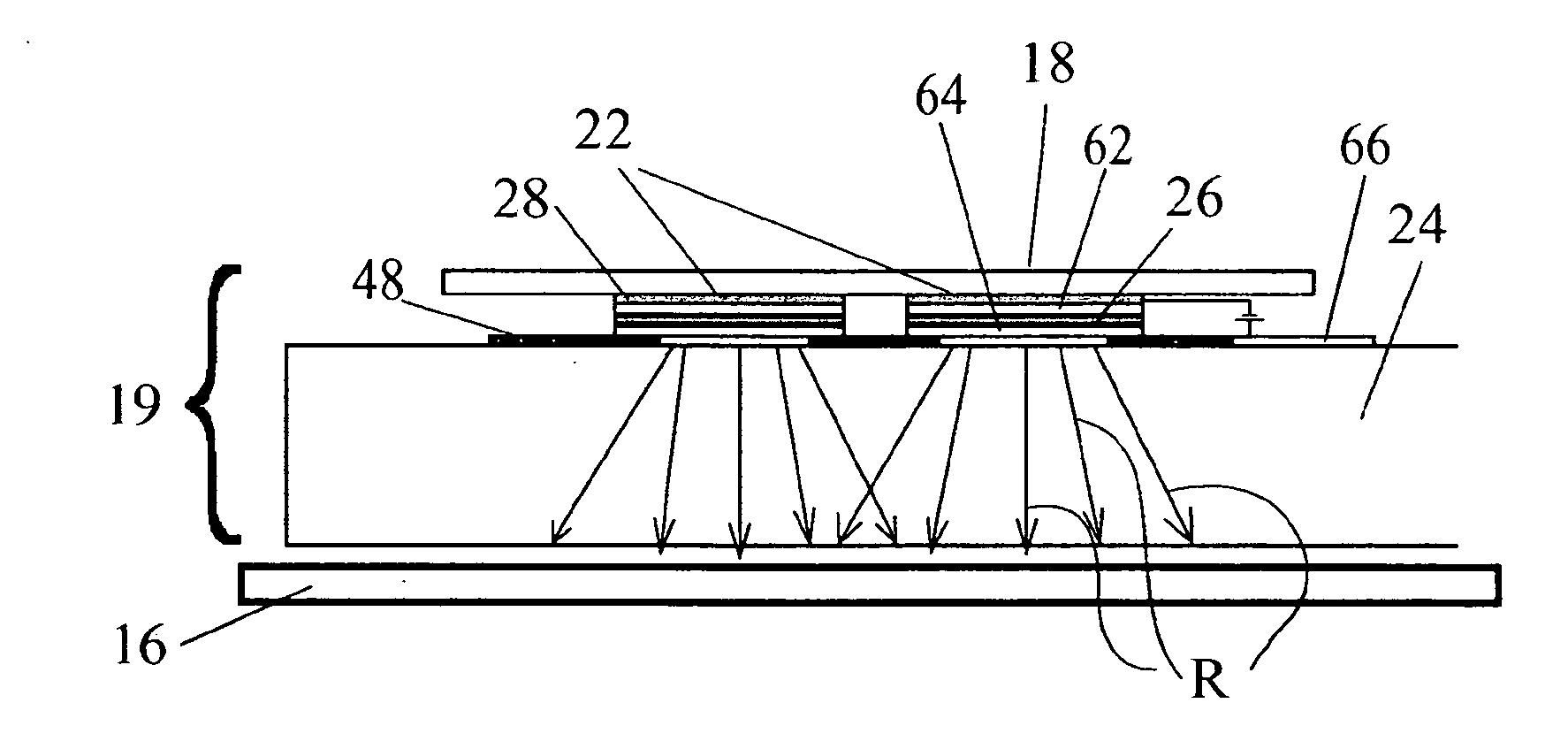
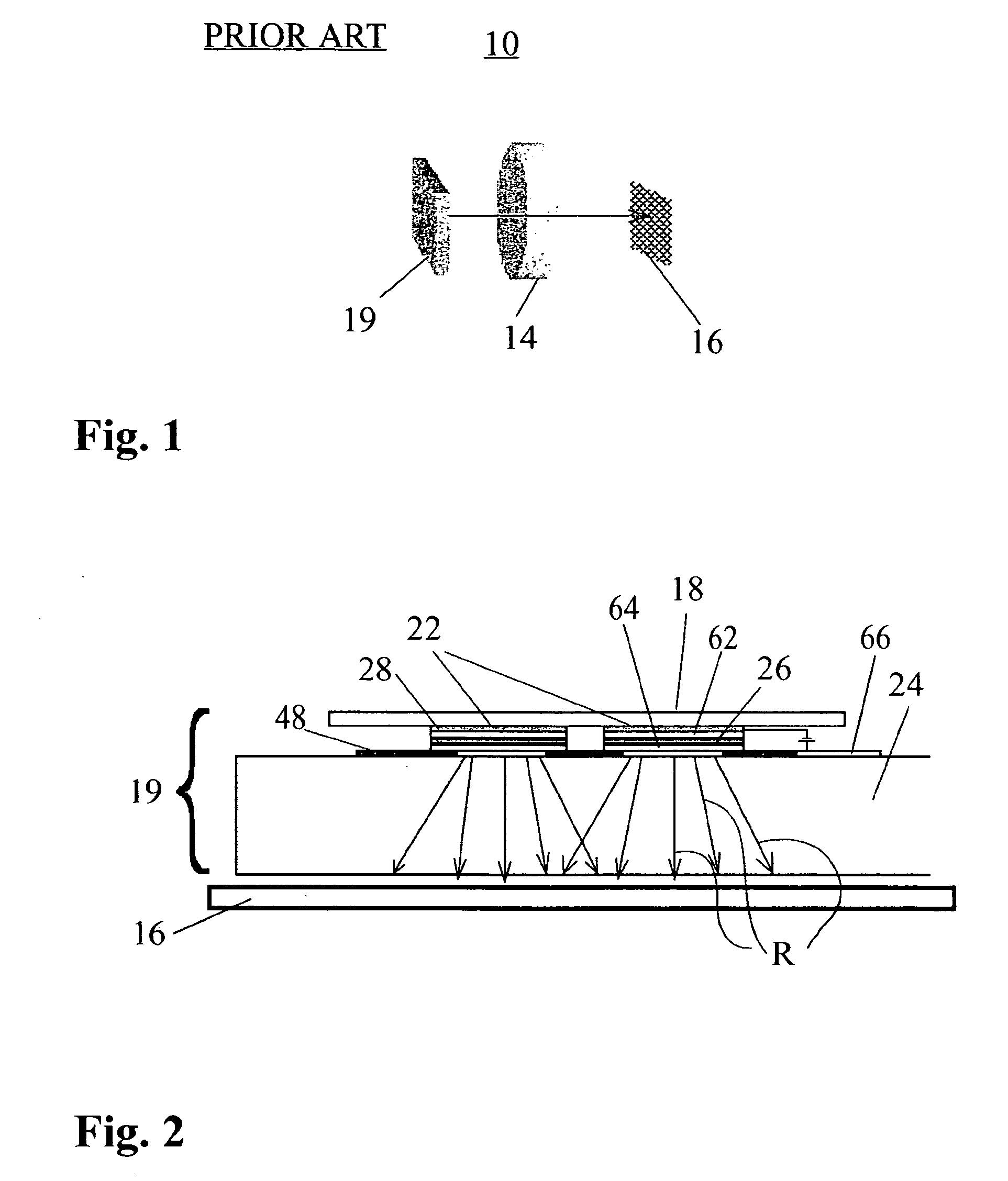
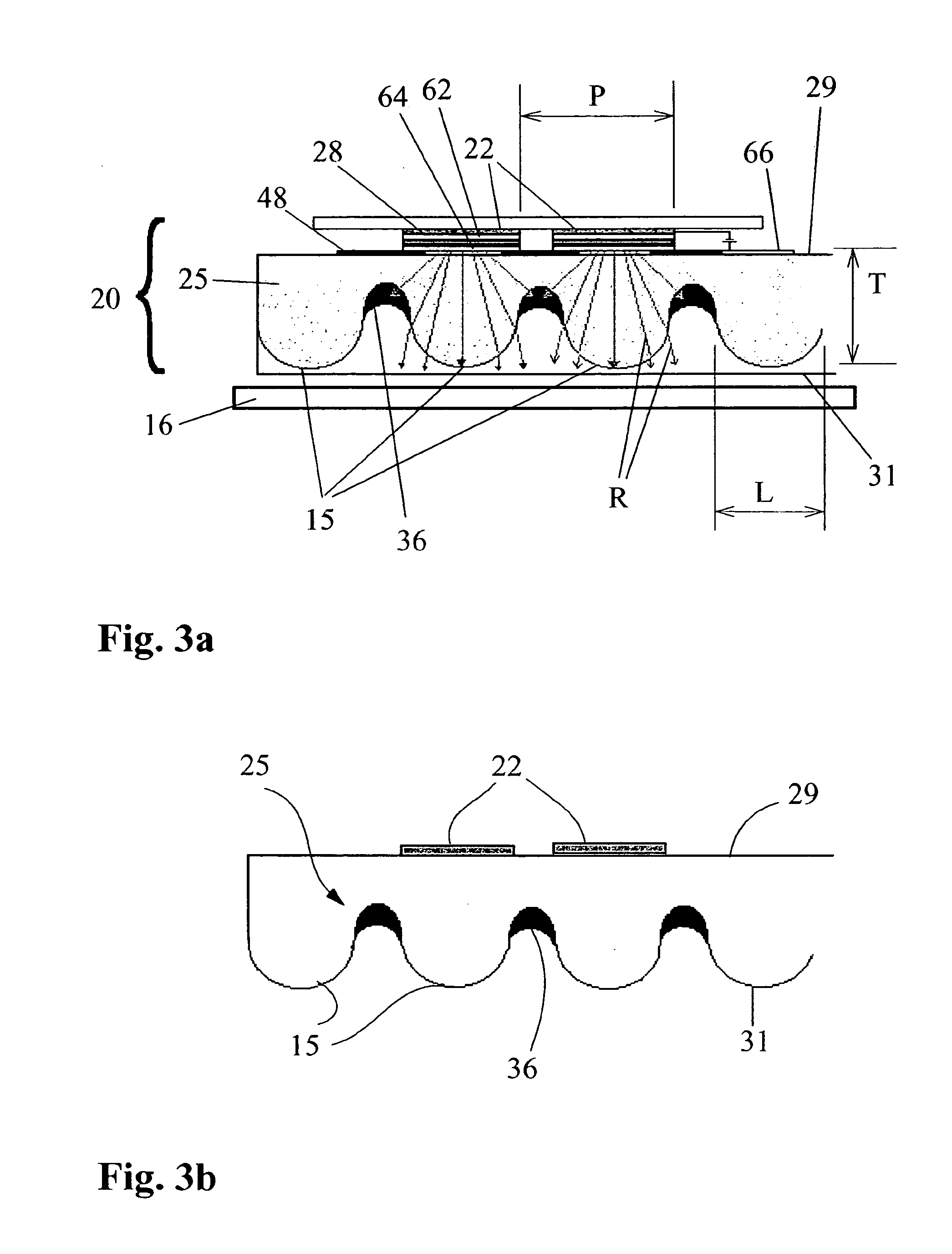
[0036] The present description is directed in particular to elements forming part of, or cooperating more directly with, apparatus in accordance with the invention. It is to be understood that elements not specifically shown or described may take various forms well known to those skilled in the art.

[0037] Photoemissive area arrays adaptable for printing applications can be constructed from a variety of materials. The preferred embodiment in the present invention makes use of organic light emitting diode (OLED) arrays, using organic electroluminscence technology. The light emitting material itself may be characterized as being of the small-molecule kind or of the polymer kind. In some of the current literature, small-molecule organic electroluminescent devices are labeled as “OLED” devices and distinguished from polymer organic electroluminescent devices, labeled “PLED” devices. For the purposes of this application, however, all of these classes of organic electroluminescent devices...


PUM


Abstract

A contact printing apparatus (100), using a direct-coupled emissive array (20) of individual light emitting pixels (22), forms an image from digital data onto a photosensitive medium (16). The direct-coupled emissive array (20) is fabricated on an optically coupled substrate (25) that provides light-directing elements, such as a lenslet array or fiber optic faceplate (40) for directing light from emitter pixels (22) to print pixel (71) locations on the photosensitive medium (16).

Description

CROSS REFERENCE TO RELATED APPLICATIONS [0001] Reference is made to commonly-assigned copending U.S. patent application Ser. No. 10 / 201,338, filed Jul. 23, 2002, entitled OLED DISPLAYS WITH FIBER-OPTIC FACEPLATES, by Cok et al., the disclosure of which is incorporated herein.FIELD OF THE INVENTION [0002] This invention generally relates to printing apparatus and more particularly relates to a printer for forming an image using a direct-coupled photoemissive array. BACKGROUND OF THE INVENTION [0003] A number of different imaging technologies have been employed for recording images from digital data onto photosensitive media. Technologies adapted for digital printing onto photosensitive media include cathode ray tube (CRT), scanned laser beam, liquid crystal display (LCD) and digital micromirror device (DMD) technologies. Each of these imaging technologies achieves some measure of success for producing high quality prints competitive with more traditional optical imaging approaches. [...

Claims


Application Information

Patent Timeline
IPC IPC(8): B41J2/45H01L51/52
CPCB41J2/45H01L51/5275H01L51/5237H01L51/52H10K50/80H10K50/841H10K50/858
Inventor WONG, VICTOR C.NARAYAN, BADHRIEVANS, GARETH B.
Owner EASTMAN KODAK CO
Why Eureka
Try Eureka