Method for forming contact plug of semiconductor device

Inactive Publication Date: 2005-11-03
SK HYNIX INC
View PDF4 Cites 15 Cited by
  • Summary
  • Abstract
  • Description
  • Claims
  • Application Information

AI Technical Summary

Benefits of technology

[0016] Accordingly, the present invention has been made to solve the above-mentioned problems occurring in the prior art, and an object of the present invention is to provide a method for forming a contact plug of a semiconductor device capable of obtaining low contact resistance and excellent refresh characteristics by using epitaxial silicon as contact material.
[0017] Another object of the present invention is to provide a method for forming a contact plug of a semiconductor device capable of growing epitaxial silicon as contact material using conventional processes without modification for easy and productive formation of epitaxial silicon.

Problems solved by technology

As semiconductor devices are highly integrated, it has become difficult to secure the characteristics of the devices.
In spite of the decrease in size of the cell transistor, downward adjustment of the operating voltage is performed very slowly and there is concern that refresh characteristics may deteriorate due to the increase in local electric field.
In summary, it has become difficult to satisfy both the operating current and the refresh characteristics of the cell transistor as the DRAM is highly integrated.
Specifically, there is a tradeoff between the operating current and the refresh characteristics of the cell transistor, and it is substantially difficult to simultaneously improve both of them.
However, such new processes are not currently adapted with ease due to the complexities of the process.
In order to grow productive film with the SEG method, however, there are many problems to be solved as follows: firstly, a dummy pattern needs to be designed due to the pattern dependence of film growth rate and thickness uniformity; secondly, proper pre-cleaning before selective epitaxial silicon growth is necessary, specifically, light etching, fluoride-based (HF, BOE, HF vapor) wet cleaning, and in-situ hydrogen bake before selective epitaxial growth are necessary; thirdly, abnormal growth on the insulating surface must be suppressed by precisely controlling contamination by metal; fourthly, there is a burden of the deterioration of characteristics of the short channel transistor caused by high-temperature (800° C. or above) in-situ hydrogen bake and epitaxial silicon growth temperature; fifthly, there is difficulty in integrating processes because of facet formation; and sixthly, if epitaxial silicon does not grow on some faulty contacts among many contacts, a problem may occur in the following process.
The SEG method also needs some special equipment technology which is hard to use.
In summary, although contact resistance may decrease and refresh may improve simultaneously when epitaxial silicon is used as cell contact landing plug material, this method cannot be easily adopted in mass production because of the above-mentioned problems.

Method used


Image

  • Method for forming contact plug of semiconductor device
  • Method for forming contact plug of semiconductor device
  • Method for forming contact plug of semiconductor device

Examples


Embodiment Construction

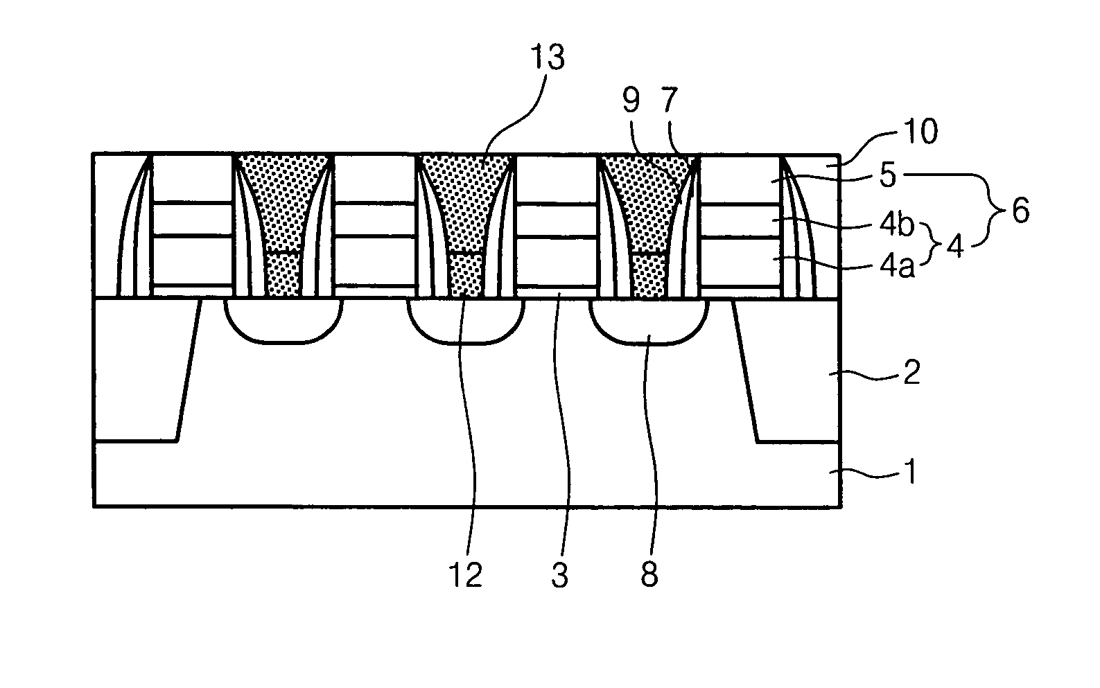
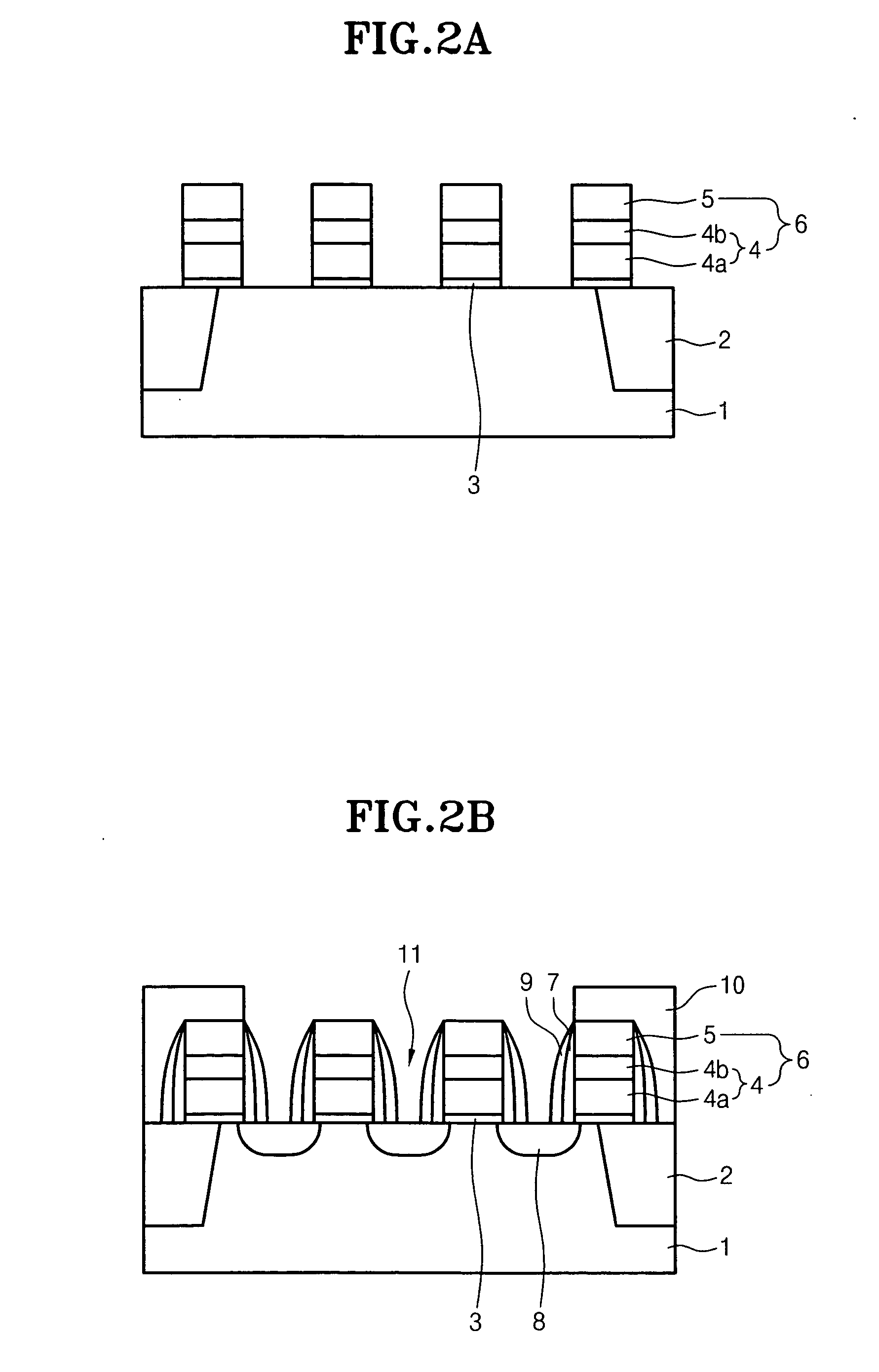
[0035] Hereinafter, a preferred embodiment of the present invention will be described with reference to the accompanying drawings. In the following description and drawings, the same reference numerals are used to designate the same or similar components, and so repetition of the description on the same or similar components will be omitted.

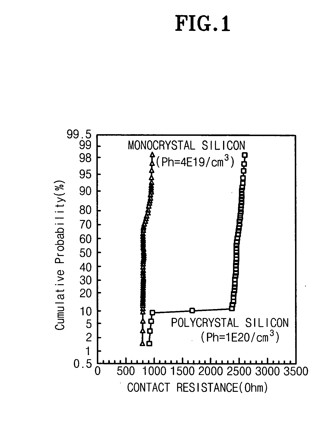
[0036] According to the present invention, epitaxial silicon is formed as contact material, i.e., as cell contact landing plug material. In order to form epitaxial silicon, a solid-phase epitaxy (hereinafter, referred to as SPE) method is used wherein amorphous silicon having a suitable range of phosphorus (P) needed by a device at low temperature is deposited on a contact interface, which has been subject to selective pre-cleaning, and epitaxial silicon is subsequently formed through re-crystallization annealing at low temperature. The present invention also makes it possible to stabilize the growth of epitaxial silicon by obtaining a contact i...


PUM


Abstract

In a method for forming a contact plug of a semiconductor device, epitaxial silicon is formed as contact material using a solid-phase epitaxy method. The method can obtain reduced contact resistance and improved refresh characteristics, compared with prior arts using polysilicon as contact material. Also, the method uses an SPE method, not a conventional SEG method, to form epitaxial silicon so that it can substantially reduce thermal budget through low-temperature processes. The method can also use conventional polysilicon deposition process without modification to form epitaxial silicon with ease and productivity.

Description

BACKGROUND OF THE INVENTION [0001] 1. Field of the invention [0002] The present invention relates to a method for forming a contact plug of a semiconductor device, and more particularly to a method for forming epitaxial silicon as contact material using a solid-phase epitaxy method. [0003] 2. Description of the Prior Art [0004] As semiconductor devices are highly integrated, it has become difficult to secure the characteristics of the devices. In the case of a DRAM cell transistor, for example, cell contact area decreases as the size of the cell transistor is gradually reduced. Consequently, a rapid increase in contact resistance followed by rapid decrease in operating current of the cell transistor is expected. In spite of the decrease in size of the cell transistor, downward adjustment of the operating voltage is performed very slowly and there is concern that refresh characteristics may deteriorate due to the increase in local electric field. In summary, it has become difficult t...

Claims


Application Information

Patent Timeline
IPC IPC(8): H01L21/28H01L21/02H01L21/20H01L21/285H01L21/336H01L21/768
CPCH01L21/02063H01L21/2022H01L21/28525H01L29/66628H01L21/76877H01L29/41783H01L29/6656H01L21/76814H01L21/02532H01L21/02667H01L21/02576H01L21/02639H01L21/0262H01L21/28H01L21/02598
Inventor LEE, SEOK KIUAHN, TAE HANGPARK, SUNG EONCHO, JUN HEEKIM, YIL WOOK
Owner SK HYNIX INC
Why Eureka
Try Eureka