

Wiring over substrate, semiconductor device, and methods for manufacturing thereof
a manufacturing method and technology for semiconductor devices, applied in the direction of printed circuit manufacturing, optics, instruments, etc., can solve the problems of deterioration of the insulating layer provided between the wiring, short circuiting or short circuiting of the wiring, and increased projection and depression difference, so as to prevent short circuiting between the wiring and the insulating layer from cracking, the effect of high yield
- Summary
- Abstract
- Description
- Claims
- Application Information
AI Technical Summary
Benefits of technology
Problems solved by technology
Method used
Image

Examples
embodiment 1
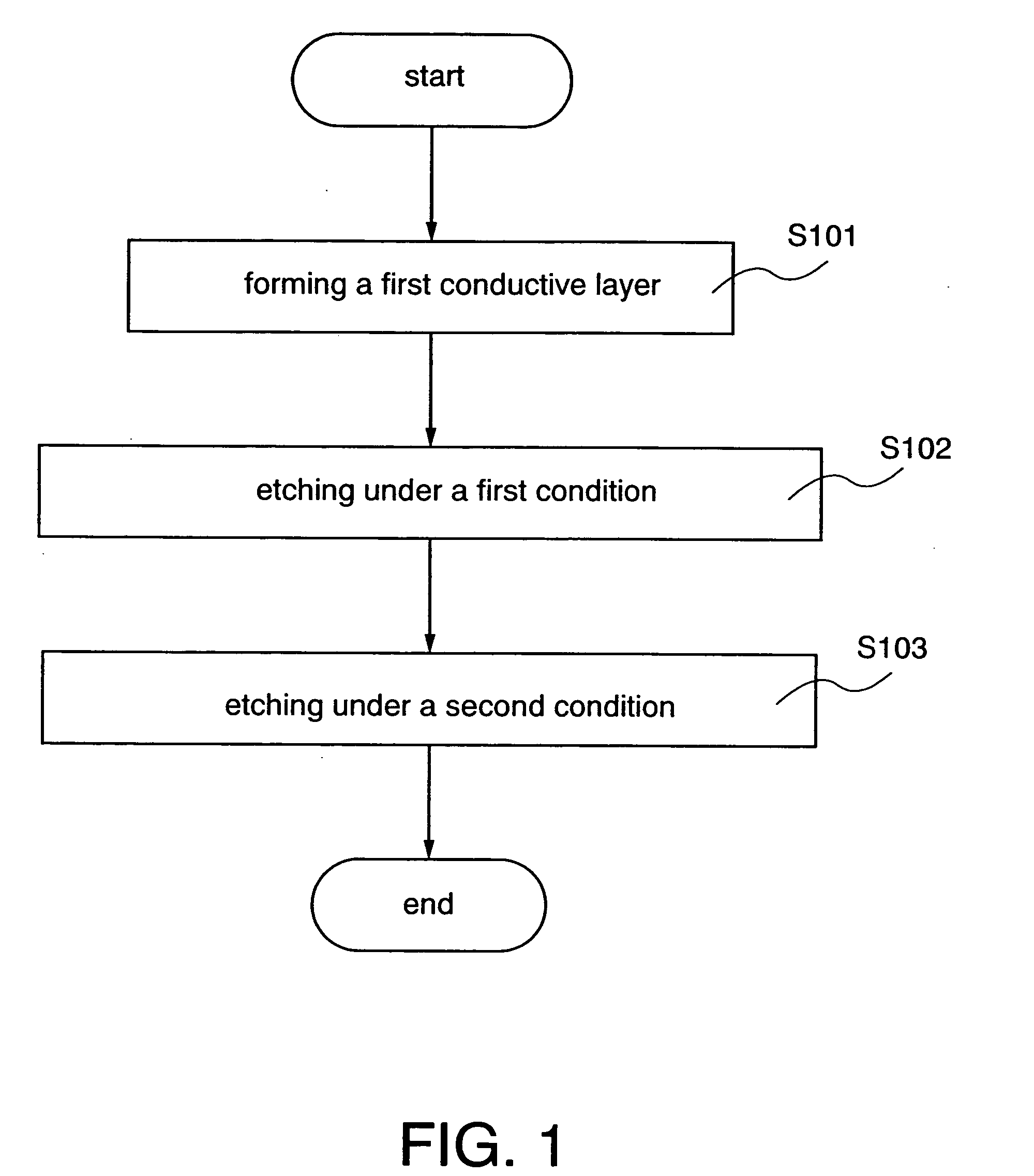
[0049] In this embodiment, a method for manufacturing a wiring over a substrate comprising a wiring having a side with a curved face by an etching process under a first condition and an etching process under a second condition is explained with reference to FIGS. 1, 3A to 3D, and 7.
[0050] As illustrated in FIG. 3A, a first insulating layer 101 is formed over a substrate 100, and a first conductive layer 102 is formed over the first insulating layer 101. Then, a first mask pattern 103 is formed over the first conductive layer 102 (a step S101 in FIG. 1).
[0051] As the substrate 100, a substrate made from an insulating material such as a glass substrate, a quartz substrate, or alumina substrate; a plastic substrate having heat resistance that can resist processing temperature in a later process; a silicon wafer; a metal plate; or the like can be used. In this instance, an insulating film for preventing dispersion of impurities from the substrate such as silicon oxide (SiOx), silicon ...
embodiment 2
[0069] In this embodiment, a method for manufacturing a wiring having a side with a curved face according to a different etching condition from that explained in Embodiment 1 is explained with reference to FIGS. 1, 4A to 4D, and 7.
[0070] As illustrated in FIG. 4A, as is the case with Embodiment 1, a first insulating layer 101 is formed over a substrate 100, and a first conductive layer 102 is formed over the first insulating layer 101. Then, a first mask pattern 103 is formed over the first conductive layer 102 (a step S101 in FIG. 1).
[0071] As illustrated in FIG. 4B, the first conductive layer 102 is etched by using the first mask pattern 103 under a first condition to form a second conductive layer 211 having a side perpendicular to the first mask pattern 103 (a step S102 in FIG. 1). The first condition is the condition by which the first conductive layer 102 is anisotropically etched, typically, a conductive layer having a perpendicular side is formed. Further typically, the fi...
embodiment 3
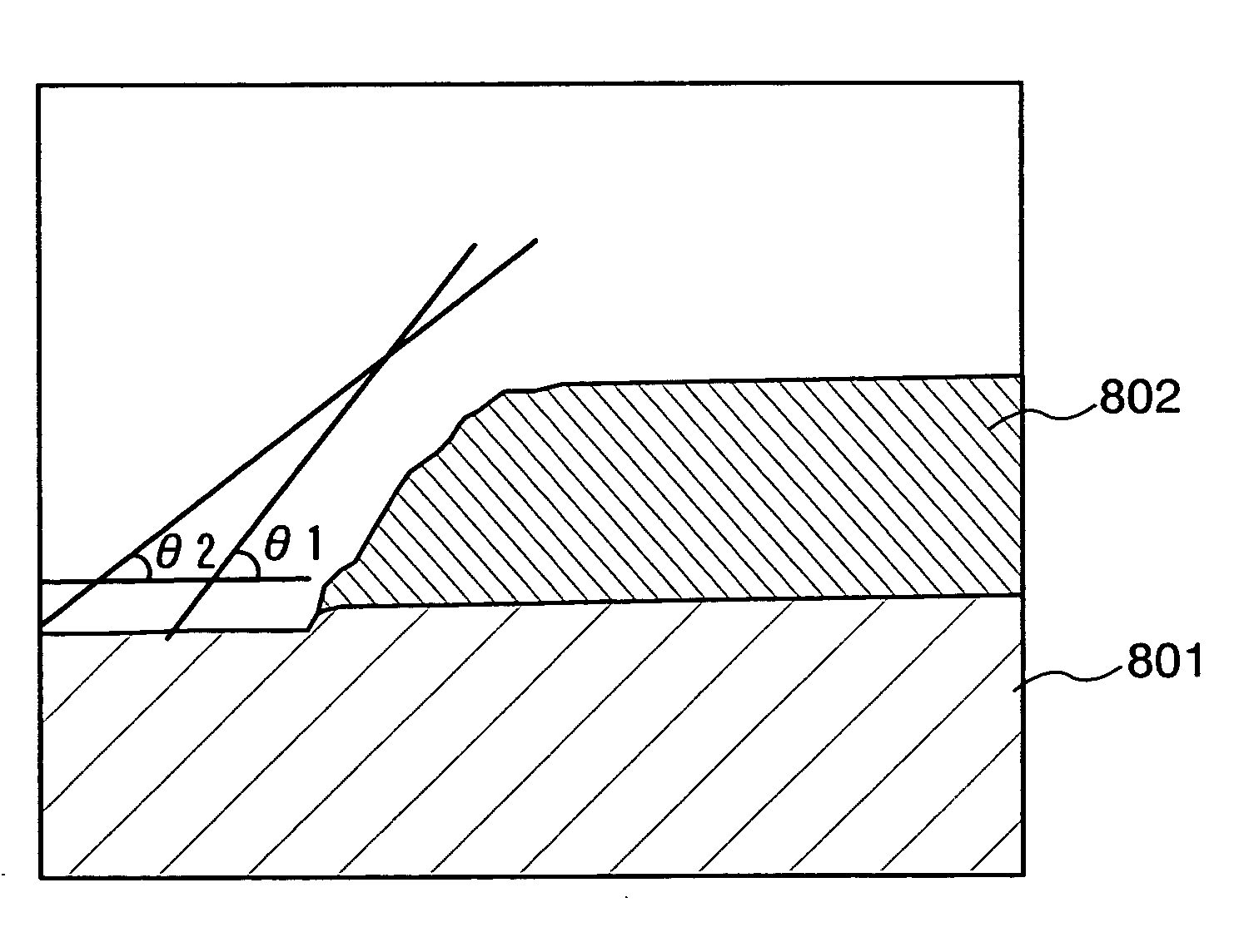
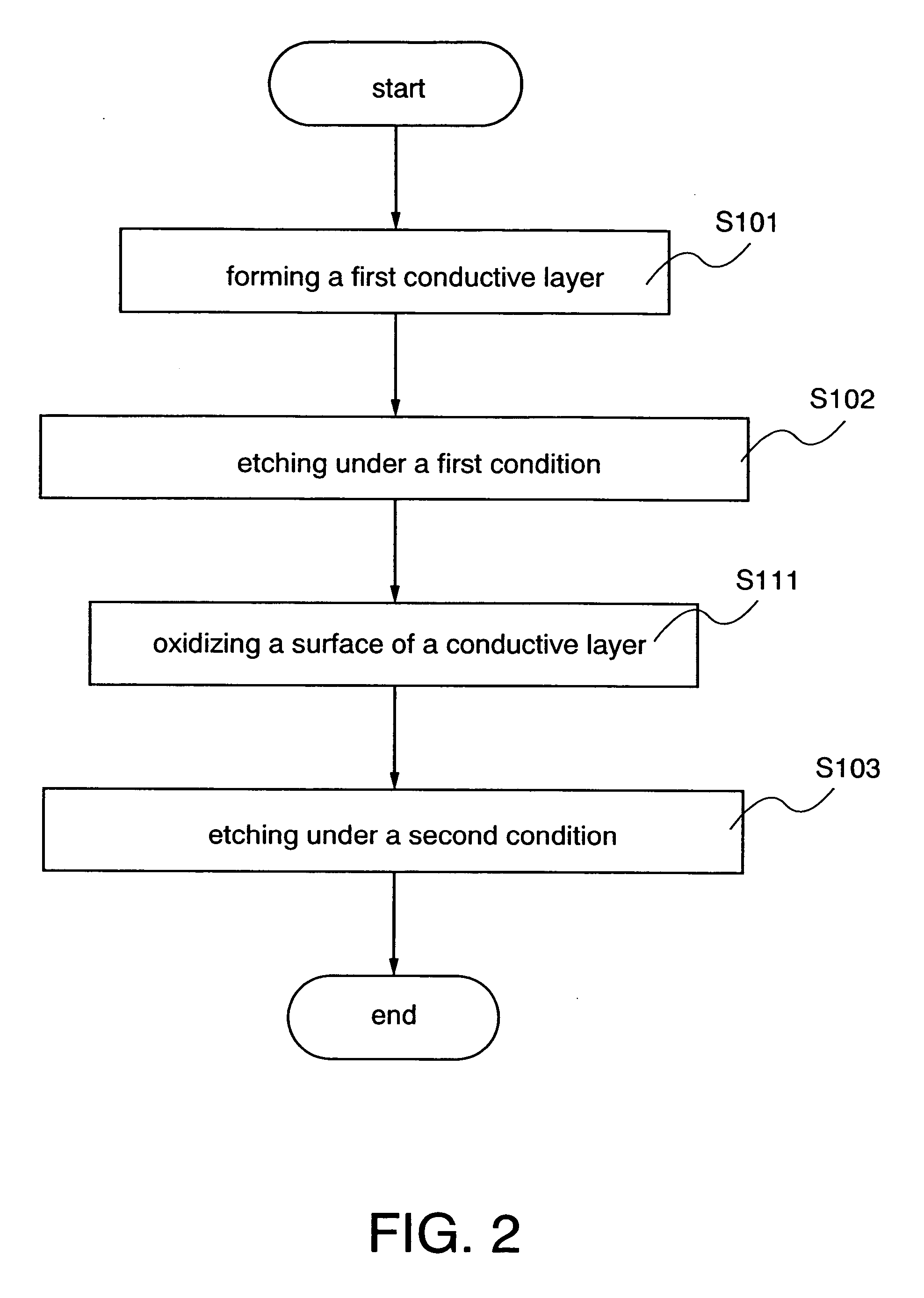
[0078] In this embodiment, a method for manufacturing a wiring having a side having a plurality of inclined planes according to a different etching process from that in Embodiments 1 and 2 is explained with reference to FIGS. 2, 5A to 5F, and 8.
[0079] As illustrated in FIG. 5A, a first insulating layer 101 is formed over a substrate 100 as is the case with Embodiment 1, and a first conductive layer 102 is formed over the first insulating layer 101. Then, a first mask pattern 103 is formed over the first conductive layer 102 (a step S101 in FIG. 2).
[0080] As illustrated in FIG. 5B, the first conductive layer 102 is etched by using the first mask pattern 103 under a first condition to form a second conductive layer 302 (a step S102 in FIG. 2). The first condition is the condition by which the first conductive layer 102 is etched, therefore, a conductive layer having a tapered edge is formed. In this instance, the first condition in this example is the same as that in Embodiment 1. N...
PUM
| Property | Measurement | Unit |
|---|---|---|
| angle of inclination | aaaaa | aaaaa |
| angle | aaaaa | aaaaa |
| angle | aaaaa | aaaaa |
Abstract
Description
Claims
Application Information