Semiconductor device

a technology of semiconductors and devices, applied in semiconductor devices, semiconductor/solid-state device details, inductances, etc., can solve the problems of only reducing electromagnetic interference, the length of the line connecting the elements becomes long, and the inductor cannot offer its intrinsic performance, so as to reduce the capacitance between the terminals of the inductor, reduce the electromagnetic interference between the inductor and other elements disposed therearound, and reduce the electromagnetic interference

Inactive Publication Date: 2005-11-10
MITSUBISHI ELECTRIC CORP
View PDF9 Cites 34 Cited by
  • Summary
  • Abstract
  • Description
  • Claims
  • Application Information

AI Technical Summary

Benefits of technology

[0013] According to a first aspect of the present invention, the semiconductor device includes: an inductor provided with a conductor interconnection formed in spiral form on a semiconductor substrate; and a shield that is provided with a continuous conductor interconnection provided along the periphery of the spiral pattern of the inductor, a portion of the conductor interconnection being opened, and that is electrically connected to ground potential. With this composition, the shield can be functioned as a return path of a high frequency signal propagating through the inductor. As a result, an electromagnetic interference between the inductor and other elements disposed around this inductor can be reduced.
[0014] Further, the above semiconductor device is arranged such that an interconnection width of the shield and a distance between the shield and the outer border of the interconnection of the inductor each are at least equal in size to a spacing of the spiral pattern of the inductor. With this composition, a capacitance between terminals of the inductor can be greatly reduced, and thereby the shield can be functioned as a return path of a high frequency signal propagating through the inductor. As a result, the electromagnetic interference between the inductor and other elements disposed therearound can be reduced.
[0015] The semiconductor device according to the present invention is arranged such that the device has a plurality of interconnection layers formed on the semiconductor substrate; the inductor is formed in any one of these interconnection layers; and the shield is formed in the same interconnection layer as and / or a different interconnection layer from the interconnection layer in which the inductor is formed. With this composition, the capacitance between the terminals of the inductor can be greatly reduced, and thereby the shield can be functioned as the return path of the high frequency signal propagating through the inductor. As a result, the electromagnetic interference between the inductor and the other elements disposed therearound can be reduced.
[0016] According to a second aspect of the present invention, the semiconductor device includes: an inductor provided with a conductor interconnection formed in spiral form on a semiconductor substrate; and a shield that is provided with a continuous conductor interconnection provided along the inner periphery of the spiral pattern of the inductor, a portion of the conductor interconnection being opened, and that is electrically connected to ground potential. With this composition, the shield can be functioned as the return path of the high frequency signal propagating through the inductor. As a result, the electromagnetic interference between the inductor and other elements disposed therearound can be reduced.
[0017] Further, this semiconductor device is arranged such that the interconnection width of the shield is at most equal to the interconnection width of the inductor. With this composition, the capacitance between the terminals of the inductor can be remarkably reduced, and thereby the shield can be functioned as the return path of the high frequency signal propagating through the inductor. As a result, the electromagnetic interference between the inductor and other elements disposed therearound can be reduced.

Problems solved by technology

In this case, the inductor cannot offer its intrinsic performance.
However, this method can only reduce the electromagnetic interference, but the length of a line connecting the elements becomes long.
Therefore, there arises another inconvenience that the line loss is increased.
Moreover, because of difficulty in size reduction of the circuit, a high degree of integration cannot be achieved.
Further, in the area of the guard ring, other elements cannot be disposed.
Accordingly, there arises an inconvenience that size reduction of the circuit in the device and a high degree of integration in the circuit cannot be achieved.
Moreover, the above-mentioned composition is effective at preventing the electromagnetic interference caused through the silicon substrate; however, it is difficult to prevent the electromagnetic interference caused in a horizontal direction to the substrate.
For this reason, there can develop the inconvenience that the circuits become easily influenced by the ground via the guard ring, and the characteristic impedance thereof is changed.
This may become a factor to deteriorate the characteristic of the inductor.
For this reason, there has been an inconvenience that a signal loss becomes large because of the parasitic effect a rising from the substrate.
However, this composition can only prevent the noise and electromagnetic interference produced through the silicon substrate; however, this composition cannot prevent the electromagnetic interference caused in a horizontal direction to the substrate.
Moreover, there is a problem that a Q-value (Quality Factor) is deteriorated by the patterned ground shield, depending on the magnitude of the inductance, and the self-resonant frequency (the frequency at which the Q-value becomes zero) reduces, thereby narrowing the applicable frequency range of the inductor for serving as the inductor.
In this composition, it is possible to define the ground electrodes provided at the sides of the inductor as the return of the high frequency signal; however, it is impossible to define the return on the side of the input terminal and the side of the output terminal of the inductor.
For this reason, there is an inconvenience that the radiation of the electromagnetic wave from the inductor cannot be suppressed, and the radiation influences other elements existing around the inductor.
As a result, there is a problem that the performance (Q-value and self-resonant frequency) of the inductor deteriorates.

Method used


Image

  • Semiconductor device
  • Semiconductor device
  • Semiconductor device

Examples


embodiment 1

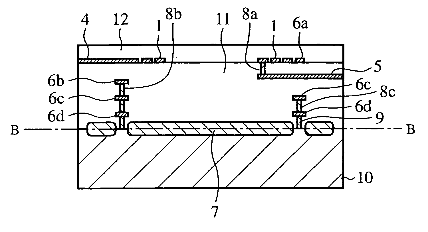
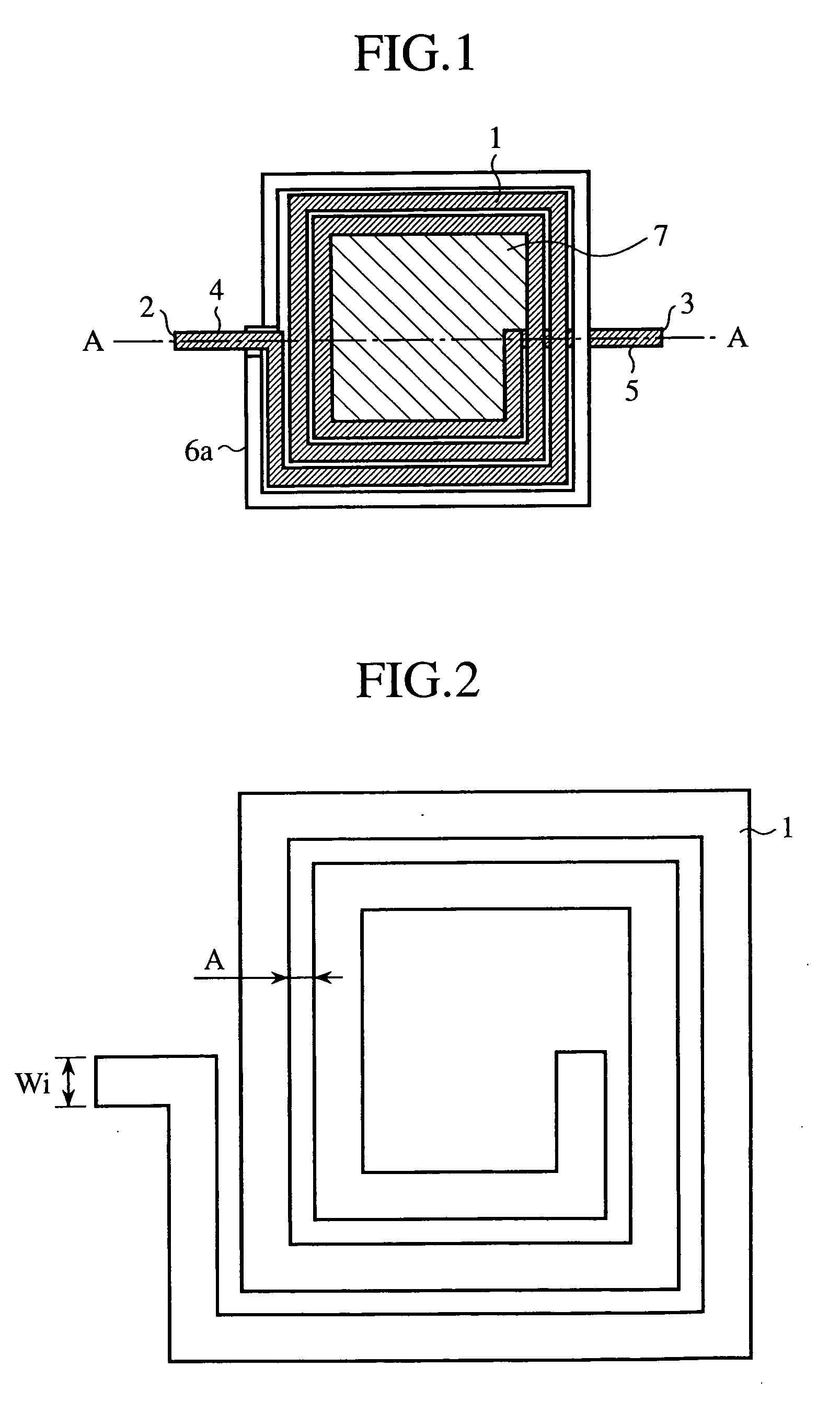
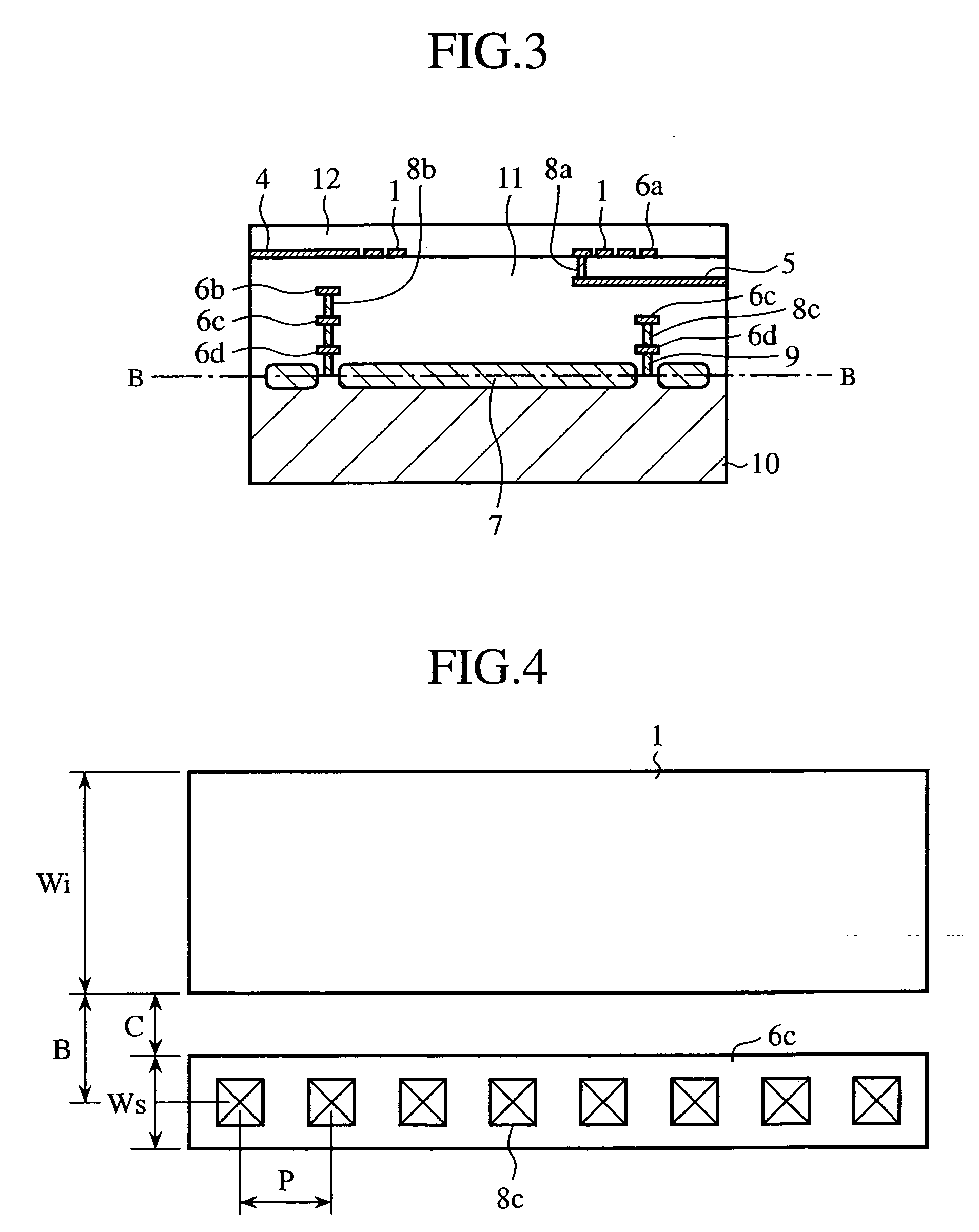
[0038]FIG. 1 is a perspective plan view of a semiconductor device in accordance with Embodiment 1 of the present invention, as seen through a passivation film and an interlayer film from above, and FIG. 2 is a top view showing the pattern of the inductor of the semiconductor device. In the semiconductor device in accordance with this embodiment, as shown in FIG. 1, a shield 6a is provided such that the shield encloses an inductor 1 formed by laying out a interconnection in a spiral form. The dimensions of the inductor 1 are, as shown in FIG. 2, such that, for example, the interconnection width Wi is 10 μm, the interconnection spacing A of the spiral pattern is 2 μm, and the number of interconnection turns of the inductor is 2.5. The high frequency signal input from an input terminal 2 is output from an output terminal 3 through a lead wire 4, the inductor 1, and a lead-out wire 5. Moreover, a trench isolation part 7 is composed of silicon oxide and so on, and electrically separates ...

embodiment 2

[0097]FIG. 14 is a perspective plan view of a semiconductor device in accordance with Embodiment 2 of the present invention, as seen through a passivation film and an interlayer film from above. FIG. 15 is a sectional view of the semiconductor device shown in FIG. 14, taken along the line D-D. As shown in FIG. 14, in the semiconductor device in accordance with this embodiment, a shield 6e is provided such that the shield encloses an inductor 1 formed by laying out a interconnection in spiral form. Herein, the dimensions of the inductor 1 are such that the interconnection width Wi thereof is 10 μm, the spacing A in the spiral pattern is 2 μm, and the number of turns therein is 2.5.

[0098] Further, as shown in FIG. 15, the semiconductor device in accordance with this embodiment has four-level aluminum interconnection layers layered on a silicon substrate 10 through insulating layers by means of a CMOS process. The inductor 1 is formed in each of the fourth aluminum interconnection lay...

embodiment 3

[0114]FIG. 17 is a perspective plan view of a semiconductor device in accordance with Embodiment 3 of the present invention, as seen through a passivation film and an interlayer film from above. The semiconductor device in accordance with this embodiment has, similarly as in Embodiments 1 and 2, four-level aluminum interconnection layers layered on a silicon substrate 10 through insulating layers by means of a CMOS process. An inductor 1 is formed in the fourth aluminum interconnection layer, which is the top layer, coated with a passivation film 12. A lead wire 4 and the inductor 1 are both formed in the fourth aluminum interconnection layer. A lead-out wire 5 is formed in the third aluminum interconnection layer, and is electrically connected with the inductor 1 formed in the fourth aluminum interconnection layer through a via hole. The high frequency signal input from an input terminal 2a is output from an output terminal 3a through the lead wire 4, the inductor 1, and the lead-o...


PUM


Abstract

A semiconductor device includes: an inductor (1) provided with a conductor interconnection formed spirally on a semiconductor substrate (10); and a shield (6a) that is provided with a continuous conductor interconnection provided along the outer periphery of the spiral pattern of the inductor (1) while opening a portion of the conductor interconnection, and that is electrically connected to ground potential.

Description

TECHNICAL FIELD [0001] The present invention relates to a semiconductor device, and more particularly relates to a semiconductor device provided with a high frequency circuit having an inductor. BACKGROUND ART [0002] A semiconductor device provided with high frequency circuits includes an inductor in addition to a resistor and a capacitor. The combination of the inductor and capacitor in action enables matching of the high frequency circuits. When a high frequency current now flows through the inductor, an electromagnetic wave is radiated from the inductor. Accordingly, when other elements (a transmission line, capacitor, resistor, and another inductor) exist around the inductor, an electromagnetic coupling (electromagnetic interference) is caused between the element and the inductor. For example, if the inductor and another inductor electromagnetically interfere with each other, a mutual inductance is caused therebetween, thereby changing the desired magnitude of inductance. In thi...

Claims


Application Information

Patent Timeline
Patent Type & Authority Applications(United States)
IPC IPC(8): H01L21/02H01L23/522H01L27/04H01L27/08
CPCH01L23/5225H01L23/5227H01L28/10H01L2924/3011H01L2924/0002H01L2924/00
Inventor NISHIKAWA, KAZUYASUHASHIZUME, YASUSHI
Owner MITSUBISHI ELECTRIC CORP
Why Eureka
Try Eureka