Organic electronic device

a technology of electronic devices and organic compounds, applied in the field of electronic devices, can solve the problems of unstable interface between electrodes and electrodes, adversely affecting the performance of electronic devices, and limitation in choosing compounds for hole injection layers,

Active Publication Date: 2005-11-17
LG DISPLAY CO LTD
View PDF15 Cites 106 Cited by
  • Summary
  • Abstract
  • Description
  • Claims
  • Application Information

AI Technical Summary

Benefits of technology

[0009] According to an aspect of the present invention, an electronic device comprises: a first electrode to inject or extract hole, the first electrode including a conductive layer and an n-type organic compound layer disposed on the conductive layer; a second electrode to inject or extract electron; and a p-type organic compound layer disposed between the n-type organic compound layer of the first electrode and the second electrode, the p-type organic compound layer forming an NP junction between the n-type organic compound layer of the first electrode and the p-type organic compound layer, wherein an energy difference between a lowest unoccupied molecular orbital (LUMO) energy of the n-type organic compound layer of the first electrode and a Fermi energy of the conductive layer of the first electrode is about 2 eV or less; and wherein an energy difference between the LUMO energy of the n-type organic compound layer of the first electrode and a highest unoccupied molecular orbital (HOMO) energy of the p-type organic compound layer is about 1 eV or less.

Problems solved by technology

The interface between electrodes having a metal, a metal oxide, or a conductive polymer, and an organic compound layer, however, is unstable.
An external heat, an internally generated heat, or the electric field applied to the electronic devices could adversely affect the performance of electronic devices.
Because the hole injection layer should be selected in view of the HOMO energy of the hole transporting layer or light emitting layer, in addition to the Fermi energy of the anode electrode, there is limitation in choosing compounds for the hole injection layer.
Compounds for anode electrode, however, are limited.
Such gold or novel metals, however, are expensive and hard to process using industrial methods, thus restricting their application and structure in organic transistors.

Method used


Image

  • Organic electronic device
  • Organic electronic device
  • Organic electronic device

Examples


example 1

Determination of HOMO and LUMO Energies of HAT with UPS and UV-VIS Absorption

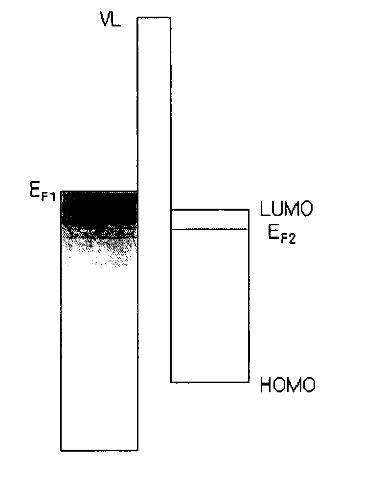
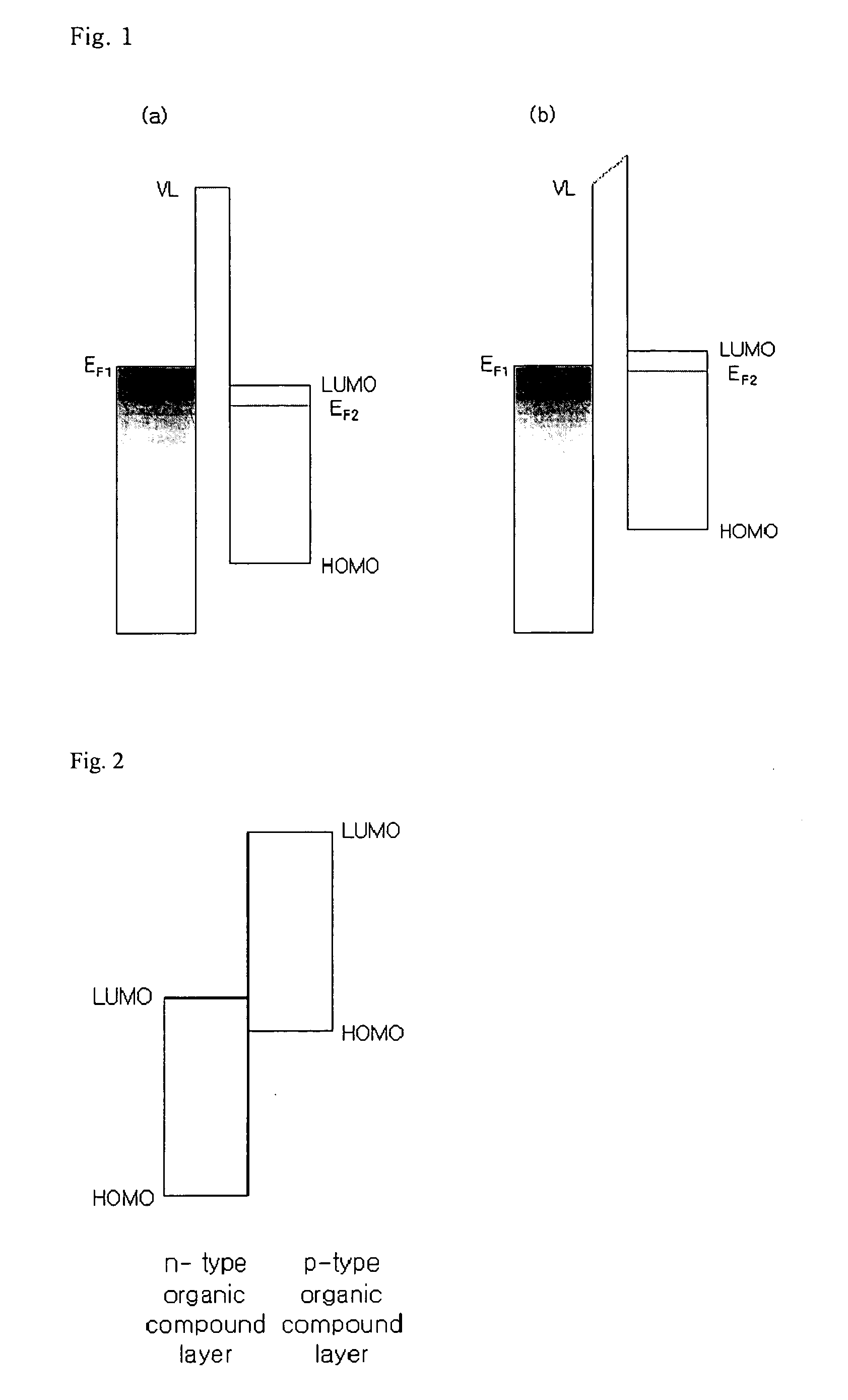
[0077] Hexanitrile hexaazatriphenylene (HAT) was used for an organic compound having n-type semiconductor property. The HOMO energy of the HAT was determined by Ultraviolet Photoelectron Spectroscopy (UPS) in which the Vacuum UV line (about 21.20 eV) emitted from a Helium lamp was illustrated to a sample under an ultra high vacuum (−10 Torr) and the kinetic energy of the electrons emitted from the sample was examined.

[0078] With the UPS, the work function of metals and the ionization energy (HOMO energy and Fermi energy) of organic compounds were determined, respectively. The kinetic energy of the emitted electrons was the energy difference between the electron binding energy of the sample and the vacuum UV energy (about 21.2 eV). Therefore, the distribution of the binding energy of the materials contained in the sample was determined by analyzing the distribution of the kinetic energy of the emitted ele...

example 2

Hole Injection Characteristic of HAT

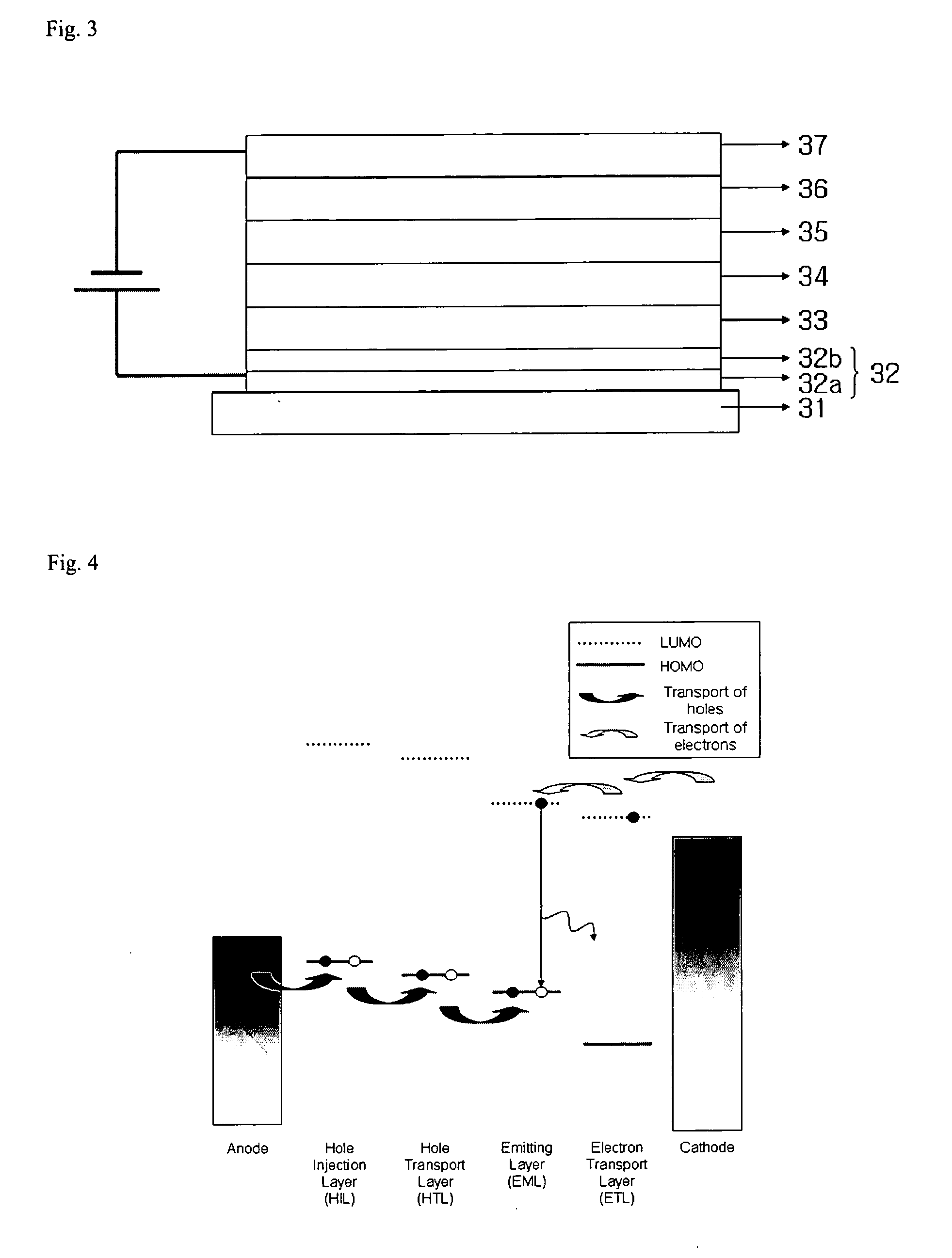
[0082] A glass substrate coated with the ITO having a thickness of 1000 Å was ultrasonic washed for thirty minutes in a distilled water in which a detergent was melted. Corning 7059 glass was used as the glass substrate, and the product 15-333-55 manufactured by Fischer Co. was used as the detergent. The glass substrate was further ultrasonically washed in the distilled water for ten minutes, which was repeated twice.

[0083] After washing, the glass substrate was sequentially ultrasonic washed for one minute in an isopropyl alcohol solvent, an acetone solvent, and a methanol solvent, and then dried. Then, the ITO coated glass substrate was treated by plasma for five minutes in a plasma cleaner by using nitrogen under a pressure of about 14 mtorr and a power of about 50 W. As a result, the work function of ITO was about 4.8 eV.

[0084] The HAT of about 100 Å was thermally deposited on the ITO electrode under vacuum to form an anode having an ITO c...

example 3

[0088] A glass substrate such as Coming 7059 glass was ultrasonically washed in a distilled water in which a detergent was dissolved. The product manufactured by Fischer Co. was used as the detergent, and the distilled water was twice filtered with the filter manufactured by Millipore Co. After washing the glass substrate for thirty minutes, the glass substrate was further ultrasonic washed in the distilled water for ten minutes, which was repeated twice.

[0089] After washing, the glass substrate was sequentially ultrasonically washed in an isopropyl alcohol solvent, an acetone solvent, and a methanol solvent, and then dried. Then, the Al having a thickness of about 500 Å was vacuum deposited on the glass substrate, and the HAT having a thickness of about 100 Å was heat and vacuum deposited on the Al conductive layer, thereby forming the anode having the Al conductive layer and the HAT n-type organic compound layer. Then, the 4,4′-bis[N-(1-naphthyl)-N-phenylamino]biphenyl (NPB) comp...


PUM

PropertyMeasurementUnit
Fermi energyaaaaaaaaaa
HOMO)aaaaaaaaaa
HOMO energyaaaaaaaaaa

Abstract

An organic electronic device. The device includes a first electrode to inject or extract hole, the first electrode including a conductive layer and an n-type organic compound layer disposed on the conductive layer, a second electrode to inject or extract electron, a p-type organic compound layer disposed between the n-type organic compound layer and the second electrode. The p-type organic compound layer forms an NP junction between the n-type organic compound layer and the p-type organic compound layer. The energy difference between a lowest unoccupied molecular orbital (LUMO) energy of the n-type organic compound layer and a Fermi energy of the conductive layer is about 2 eV or less, and the energy difference between the LUMO energy of the n-type organic compound layer and a highest unoccupied molecular orbital (HOMO) energy of the p-type organic compound layer is about 1 eV or less.

Description

[0001] This application claims the benefit of Korean Patent Application No. 10-2004-0033045, filed on May 11, 2004, in the Korean Intellectual Property Office, the disclosure of which is incorporated herein in its entirety by reference. BACKGROUND OF THE INVENTION [0002] 1. Field of the Invention [0003] The present invention relates to electronic devices having an n-type organic compound layer in an electrode for hole injection or hole extraction. More particularly, the present invention relates to electronic devices capable of lowering the energy barriers for hole injection or hole extraction. [0004] 2. Description of the Related Art [0005] Electronic devices such as solar batteries, organic luminescence devices, or organic transistors include two electrodes and an organic compound disposed between the electrodes. Solar batteries, for example, generate electricity by using the electrons and holes separated from exciton generated in organic compound layers in response to solar energ...

Claims


Application Information

Patent Timeline
Patent Type & Authority Applications(United States)
IPC IPC(8): B32B19/00H01L51/05H01L51/52
CPCB82Y10/00Y02E10/549H01L51/0052H01L51/0053H01L51/0062H01L51/0072H01L51/0081H01L51/0508H01L51/0562H01L51/424H01L51/441H01L51/5088H01L51/5206H01L51/5278H01L2251/308H01L2251/552H01L51/0046H10K85/211H10K85/621H10K85/615H10K85/649H10K85/6572H10K85/324H10K10/46H10K10/486H10K30/20H10K30/81H10K50/00H10K50/11H10K2101/40H10K50/17H10K50/81H10K50/818H10K50/19H10K2102/103H10K2101/30H05B33/14
Inventor KANG, MINSOOSON, SAE HWANCHOI, HYEONJANG, JUN GIJEON, SANG YOUNGKIM, YEON HWANYOON, SEOKHEEHAN, YOUNG KYU
Owner LG DISPLAY CO LTD
Why Eureka
Try Eureka