High performance strained channel mosfets by coupled stress effects

a mosfet and coupled stress technology, applied in the direction of basic electric elements, electrical apparatus, semiconductor devices, etc., can solve the problems of inability to achieve the desired effect of reducing the performance of the nmos and the pmos device, and affecting the performance of the pmos device. , to achieve the effect of improving degrading the performance of the pmos devi

Inactive Publication Date: 2005-11-24
TAIWAN SEMICON MFG CO LTD
View PDF8 Cites 79 Cited by
  • Summary
  • Abstract
  • Description
  • Claims
  • Application Information

AI Technical Summary

Benefits of technology

[0012] To achieve the foregoing and other objects, and in accordance with the purposes of the present invention, as embodied and broadly described herein, the present invention provides strained channel transistors including a PMOS and NMOS device pair to improve an NMOS device performance without substantially degrading PMOS device performance and method for forming the same.

Problems solved by technology

However, several shortcomings are associated with this approach including issues such as cost and process integration issues related to scalability and acceptable manufacture and performance of conventional CMOS device structures such as shallow trench isolation (STI) structures.
In this approach, the degree of strain induced in the channel region is limited by the size of the offset spacer which is dictated by design requirements of source / drain formation.
Another problem with prior art channel stressing techniques include the opposing effects on NMOS and PMOS device performance in introducing localized mechanical stresses to strain a channel region.
As a result, unacceptable trade-offs between NMOS and PMOS performance is necessary in prior art channel strain inducing techniques.
As a result, the nitride contact etching stop layer may be severely damaged, which can have the effect of undesirably changing etching rates and causing unintentional overetching in subsequent contact formation processes, for example causing damage to underlying silicon or polysilicon portions of a CMOS device thereby degrading device performance and reliability.
The prior art approaches in general, suffer from manufacturing cost, process integration issues and difficulty in producing acceptable device quality to achieve desired device performance and reliability.

Method used


Image

  • High performance strained channel mosfets by coupled stress effects
  • High performance strained channel mosfets by coupled stress effects
  • High performance strained channel mosfets by coupled stress effects

Examples


Embodiment Construction

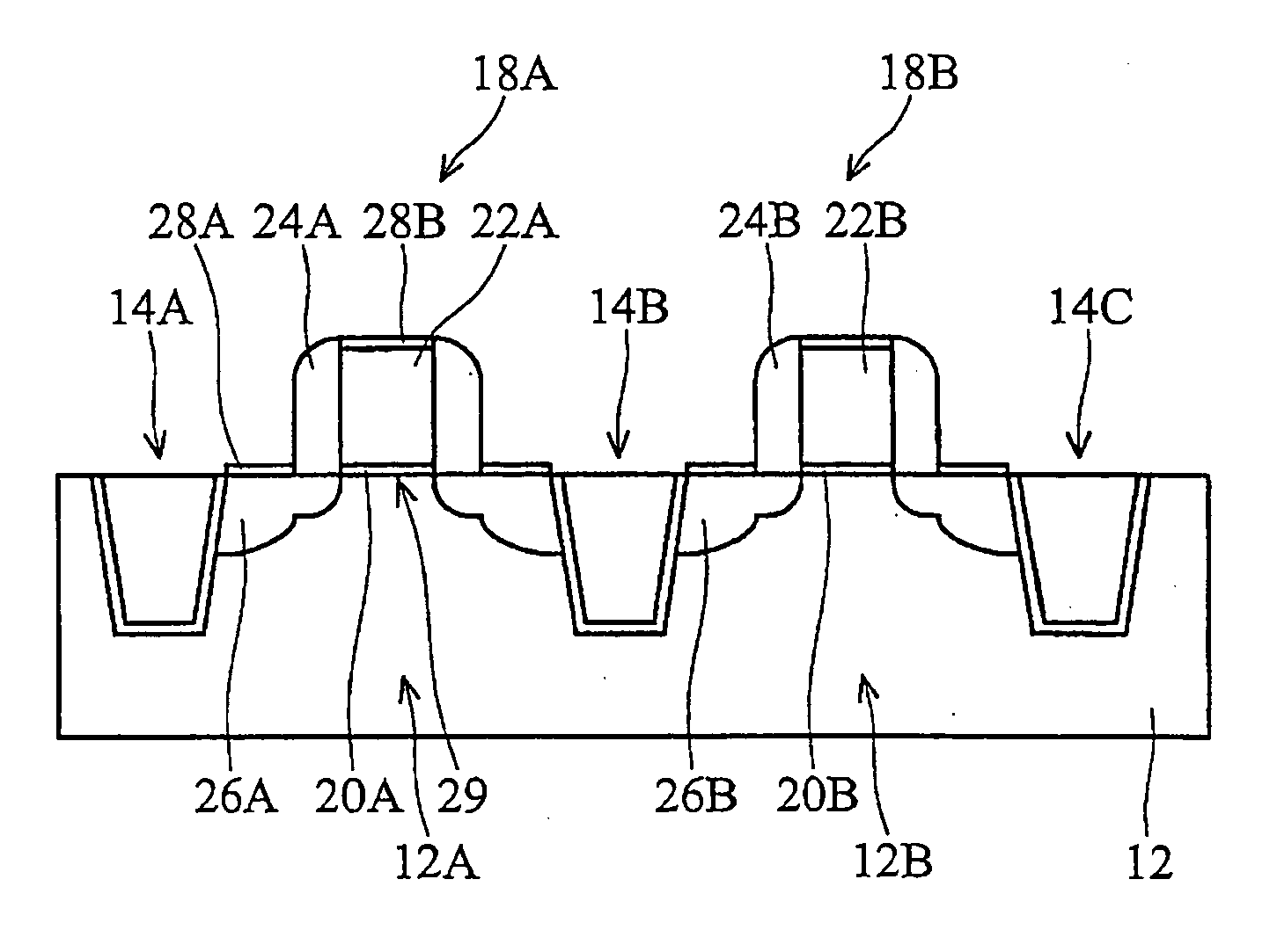
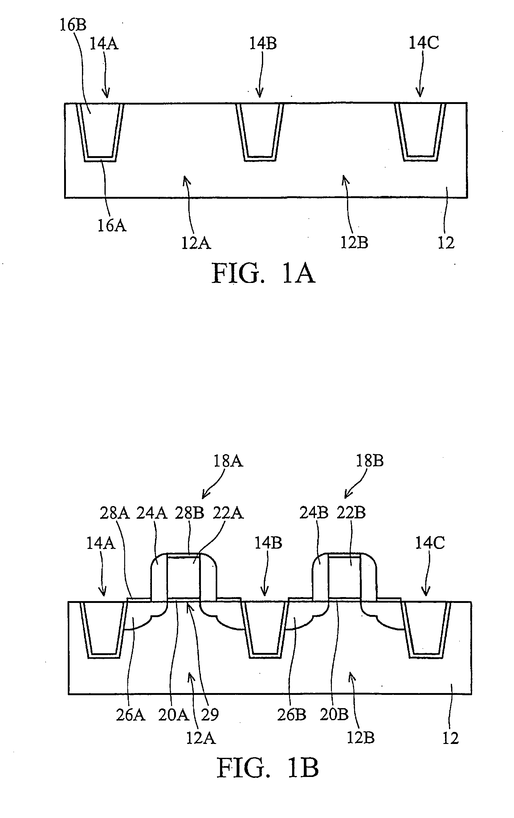
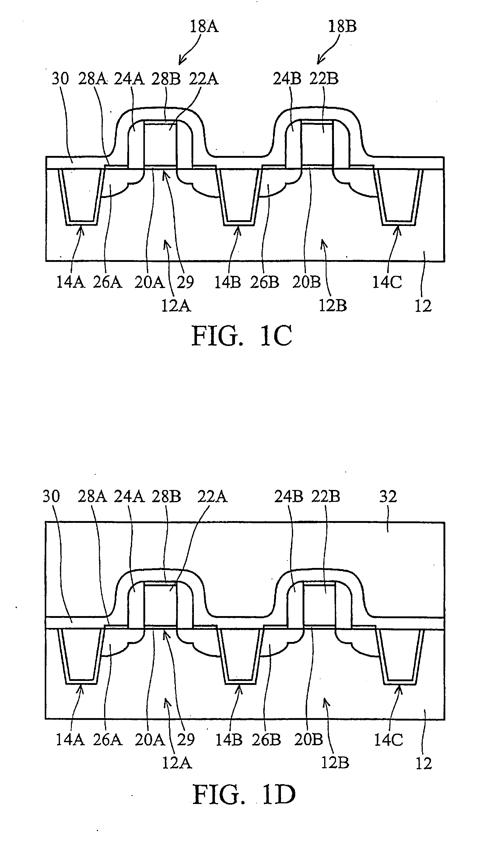
[0017] Although the method of the present invention is explained with reference to exemplary NMOS and PMOS MOSFET devices, it will be appreciated that aspects of the present invention may be applied to the formation of any MOSFET device whereby a plurality of locally mechanically induced stresses in front-end-of-line (FEOL) processes are selectively coupled to produce an improved performance of both NMOS and PMOS devices including improved drive current (Idrive)

[0018] Referring to FIGS. 1A-1E in an exemplary process flow for forming the MOSFETS of the present invention, are shown cross-sectional schematic views of a portion of a semiconductor wafer at stages of an exemplary integrated circuit manufacturing process.

[0019] For example, referring to FIG. 1A, is shown a semiconductor substrate 12, which may include silicon, strained semiconductor, compound semiconductor, multi-layered semiconductors, or combinations thereof. For example, the substrate 12 may include, but is not limite...


PUM


Abstract

Strained channel transistors including a PMOS and NMOS device pair to improve an NMOS device performance without substantially degrading PMOS device performance and method for forming the same, the method including providing a semiconductor substrate; forming strained shallow trench isolation regions in the semiconductor substrate; forming PMOS and NMOS devices on the semiconductor substrate including doped source and drain regions; forming a tensile strained contact etching stop layer (CESL) over the PMOS and NMOS devices; and, forming a tensile strained dielectric insulating layer over the CESL layer.

Description

FIELD OF THE INVENTION [0001] This invention generally relates to formation of MOSFET devices by integrated circuit manufacturing processes and more particularly to strained channel MOSFET devices and method of forming the same to improve both NMOS and PMOS performance by coupled effects of stressed dielectric layer portions. BACKGROUND OF THE INVENTION [0002] As is well known, increased device density, together with higher speed performance and lower power consumption are major driving forces in improving integrated circuit manufacturing devices and methods. For example, CMOS design considerations for high speed digital applications are usually determined by the pull up time and pull down time of each individual gate. Individual gates are associated with a delay time period for signal propagation in PMOS and NMOS gate electrodes. The delay time period, in turn, is inversely proportional to the drive current (Idrive). It is therefore clear that maximizing the drive current will incr...

Claims


Application Information

Patent Timeline
Patent Type & Authority Applications(United States)
IPC IPC(8): H01L21/8238
CPCH01L21/823807H01L21/823828H01L21/823878H01L29/7846H01L29/7843H01L29/7845H01L29/7842
Inventor CHANG, CHENG-HUNGCHANG, WENGFU, CHU-YUN
Owner TAIWAN SEMICON MFG CO LTD
Why Eureka
Try Eureka