Semiconductor package, method of production of same, and semiconductor device

a semiconductor and semiconductor technology, applied in the direction of printed capacitor incorporation, printed circuit non-printed electric component association, printed capacitor incorporation, etc., can solve the problems of switching noise, increased frequency, and increased frequency, and achieve the effect of reducing the size and weight of the package and improving the proximity degr

Inactive Publication Date: 2005-12-01
SHINKO ELECTRIC IND CO LTD
View PDF11 Cites 27 Cited by
  • Summary
  • Abstract
  • Description
  • Claims
  • Application Information

AI Technical Summary

Benefits of technology

[0010] An object of the present invention is to solve the above problems in the related art and provide a semiconductor package securing a degree of freedom of design of the interconnect patterns, greatly improving the degree of proximity between the capacitor and semiconductor chip, and enabling a reduction in size and weight of the package, a method of production of the same, and a semiconductor device using the semiconductor package.
[0013] As the high dielectric constant inorganic filler, it is most advantageous to use a powder of ceramic having a perovskite structure.

Problems solved by technology

In particular, in the case of a semiconductor package mounting a high frequency semiconductor chip required for high speed switching operations, crosstalk noise occurs more easily along with a rise in the frequency.
Further, high speed on / off operations of switching elements also cause switching noise.
The method of the related art, however, suffered from the following problems.
Further, if the interconnect distance connecting a chip capacitor and semiconductor chip is long, the inductance becomes larger and the decoupling effect of the chip capacitor can no longer be obtained.
The size of the chip capacitor etc., however, restricts the mounting position, so there were also limits to the proximity of arrangement with respect to the semiconductor chip.
Further, if mounting a chip capacitor or other capacitor in a semiconductor package, the package unavoidably becomes larger in size and heavier in weight.

Method used


Image

  • Semiconductor package, method of production of same, and semiconductor device
  • Semiconductor package, method of production of same, and semiconductor device
  • Semiconductor package, method of production of same, and semiconductor device

Examples


first embodiment

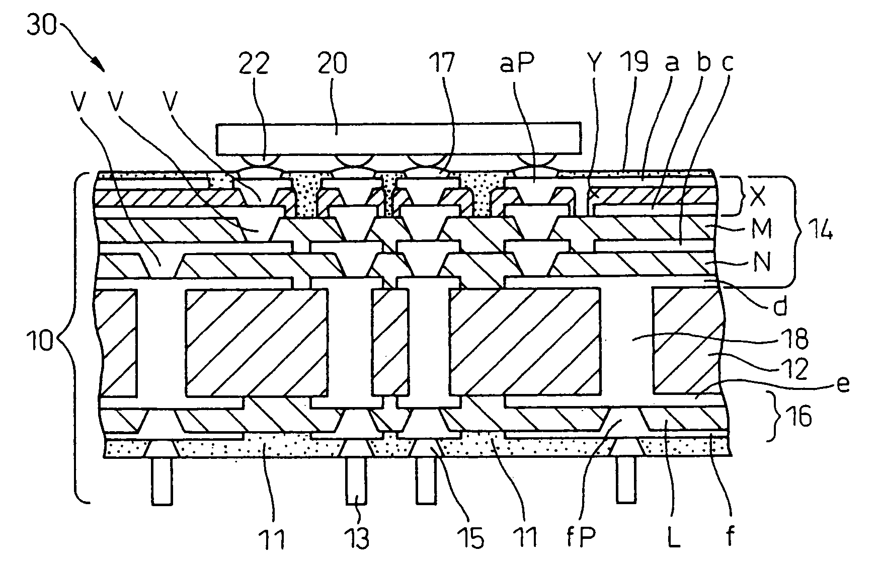
[0059]FIG. 1 is a partial sectional view of a semiconductor device 30 according to the present invention comprised of a semiconductor package 10 according to a first aspect of the present invention and a semiconductor chip 20 mounted in the same.

[0060] The semiconductor package 10 according to the first aspect of the invention is provided with a multilayer interconnect structure 14 stacked on the top surface of an insulating substrate 12, a bottom surface interconnect structure 16 formed on the bottom surface of the insulating substrate 12, and through holes 18 electrically connecting a bottommost layer “d” of the multilayer interconnect structure 14 and topmost layer “e” of the bottom surface interconnect structure 16 through the insulating substrate 12.

[0061] The bottom surface interconnect structure 16 is a structure of two interconnect layers “e” and “f” stacked via an insulating layer L. Predetermined locations of the bottommost interconnect layer “f” are formed as outside co...

second embodiment

[0099]FIG. 12 is a partial sectional view of a semiconductor device 60 according to the present invention comprised of a semiconductor package 40 according to the first aspect of the invention and a semiconductor chip 50 mounted on the same.

[0100] The semiconductor package 40 is comprised of a multilayer interconnect structure 44, semiconductor chip connection terminals comprised of solder 48 at the top surface, and outside connection terminals comprised of solder 43 of the bottom surface. The bottom surface is covered by the solder resist 41 except at the positions of the solder 43.

[0101] The multilayer interconnect structure 44 is comprised of three interconnect layers “i”, “j”, and “k” stacked via a dielectric layer “y” or insulating layers “m” and “n”. The interconnects “i” to “k” are electrically connected by vias V passing through the insulating layers “m” and “n” at the necessary locations.

[0102] The characterizing feature of the first aspect of the invention is that the m...

third embodiment

[0142]FIG. 29 is a partial sectional view of a semiconductor device 130 according to the present invention comprised of a semiconductor package 110 according to the second aspect of the invention and a semiconductor chip 120 mounted on it.

[0143] The semiconductor package 110 according to the second aspect of the invention is comprised of an insulating substrate 112 on the top and bottom surfaces of which multilayer interconnect structures 114 and 116 are provided. Through holes 118 are provided passing through the insulating substrate 112 to electrically connect the bottommost layer a4 of the top surface multilayer interconnect structure 114 and the topmost layer a5 of the bottom surface multilayer interconnect structure 116.

[0144] The aim of the structure is to prevent the occurrence of warping of the substrate in the process of production by constantly keeping the number of layers stacked on the two surfaces of the insulating substrate constant by successively building up the mu...


PUM


Abstract

A semiconductor package, provided with a multilayer interconnect structure, for mounting a semiconductor chip on its top surface, wherein a topmost stacked structure of the multilayer interconnect structure includes a capacitor structure, the capacitor structure having a dielectric layer comprised of a mixed electrodeposited layer of high dielectric constant inorganic filler and insulating resin and including chip connection pads for directly connecting top electrodes and bottom electrodes with electrodes of the semiconductor chip, whereby greater freedom in design of interconnect patterns can be secured, the degree of proximity of the capacitor and semiconductor chip can be greatly improved, and the package can be made smaller and lighter in weight, a method of production of the same, and a semiconductor device using this semiconductor package.

Description

BACKGROUND OF THE INVENTION [0001] 1. Field of the Invention [0002] The present invention relates to a package for mounting a semiconductor chip, that is, a semiconductor package, a method of production of the same, and a semiconductor device comprised of that semiconductor package and a semiconductor chip mounted in it. [0003] 2. Description of the Related Art [0004] Semiconductor devices are being made increasingly denser in many applications. In accordance with this, when providing interconnect patterns in close proximity, it is important to prevent crosstalk noise between interconnects and fluctuations in potential of power lines etc. In particular, in the case of a semiconductor package mounting a high frequency semiconductor chip required for high speed switching operations, crosstalk noise occurs more easily along with a rise in the frequency. Further, high speed on / off operations of switching elements also cause switching noise. Due to this, the potential of the power lines ...

Claims


Application Information

Patent Timeline
Patent Type & Authority Applications(United States)
IPC IPC(8): H01L23/498H05K1/11H01L23/12H05K1/16H05K3/46
CPCH01L23/49822H01L23/49833H05K1/112H05K1/162H05K3/4602H01L2924/15312H05K2201/0209H05K2201/09763H05K2203/135H01L2224/16225H01L2924/15311H05K2201/0187H01L2224/05573H01L2224/05568H01L2924/00014H01L2224/05599H01L23/12
Inventor SHIMIZU, NORIYOSHIROKUGAWA, AKIOIIJIMA, TAKAHIRO
Owner SHINKO ELECTRIC IND CO LTD
Why Eureka
Try Eureka