Vacuum apparatus including a particle monitoring unit, particle monitoring method and program, and window member for use in the particle monitoring

a vacuum apparatus and particle monitoring technology, applied in the field of vacuum apparatus, can solve the problems of reducing the operating time, increasing the cost of the semiconductor manufacturing apparatus b>800/b>, and reducing the yield, so as to achieve the effect of enhancing positively reducing the frequency of replacement, and efficiently exhibiting the resistance to active molecules

Active Publication Date: 2005-12-08
TOKYO ELECTRON LTD
View PDF16 Cites 24 Cited by
  • Summary
  • Abstract
  • Description
  • Claims
  • Application Information

AI Technical Summary

Benefits of technology

[0054] In claim 25, the window member of any one of claims 17 to 24 is characterized in that the thickness of the surface treatment layer ranges from 100 nm to 10 μm. Since the thickness of the surface treatment layer ranges from 100 nm to 10 μm, the resistance to the active molecules can be enhanced.
[0055] In claim 26, the window member of any one of claims 17 to 25 is characterized in that the base is formed of glass containing silicon as a primary component, and the surface treatment layer is exposed to active molecules included in a gas within the housing. In this way, since the base is formed of glass containing silicon as a primary component, and the surface treatment layer is exposed to active molecules included in a gas within the housing, the surface treatment layer can more efficiently exhibit the resistance to the active molecules while preventing the silicon from being exposed to the plasma atmosphere, thereby positively reducing the frequency of replacement.

Problems solved by technology

If particles generated during a manufacturing processing adhere to product wafers, the wafers would be contaminated, resulting in reduction in yield.
Consequently, costs of the semiconductor manufacturing apparatus 800 are increased, while its operating time decreases.
The deposits might come apart from the inner wall of the processing chamber 810 during the manufacturing process and the like, resulting in a contamination of the wafer.
In addition, when heating the quartz glass of the window member to prevent the deterioration thereof, a defect may be caused in an electric circuit disposed within the semiconductor manufacturing apparatus800 or deterioration of a laser unit may be accelerated.
Furthermore, with regard to the above techniques for allowing a member to contain aluminum therein, since aluminum atoms are dispersed in silica or quartz, the surface of the member cannot exhibit plasma resistance or resistance to active molecules efficiently, so that the frequency of replacing the member increases.
As a result, the time required for the replacement work increases, which in turn results in deterioration in the productivity of the semiconductor manufacturing apparatus 800.
Moreover, due to the increase of costs for the replacements, overall costs of the semiconductor manufacturing apparatus 800 rises.

Method used


Image

  • Vacuum apparatus including a particle monitoring unit, particle monitoring method and program, and window member for use in the particle monitoring
  • Vacuum apparatus including a particle monitoring unit, particle monitoring method and program, and window member for use in the particle monitoring
  • Vacuum apparatus including a particle monitoring unit, particle monitoring method and program, and window member for use in the particle monitoring

Examples


first embodiment

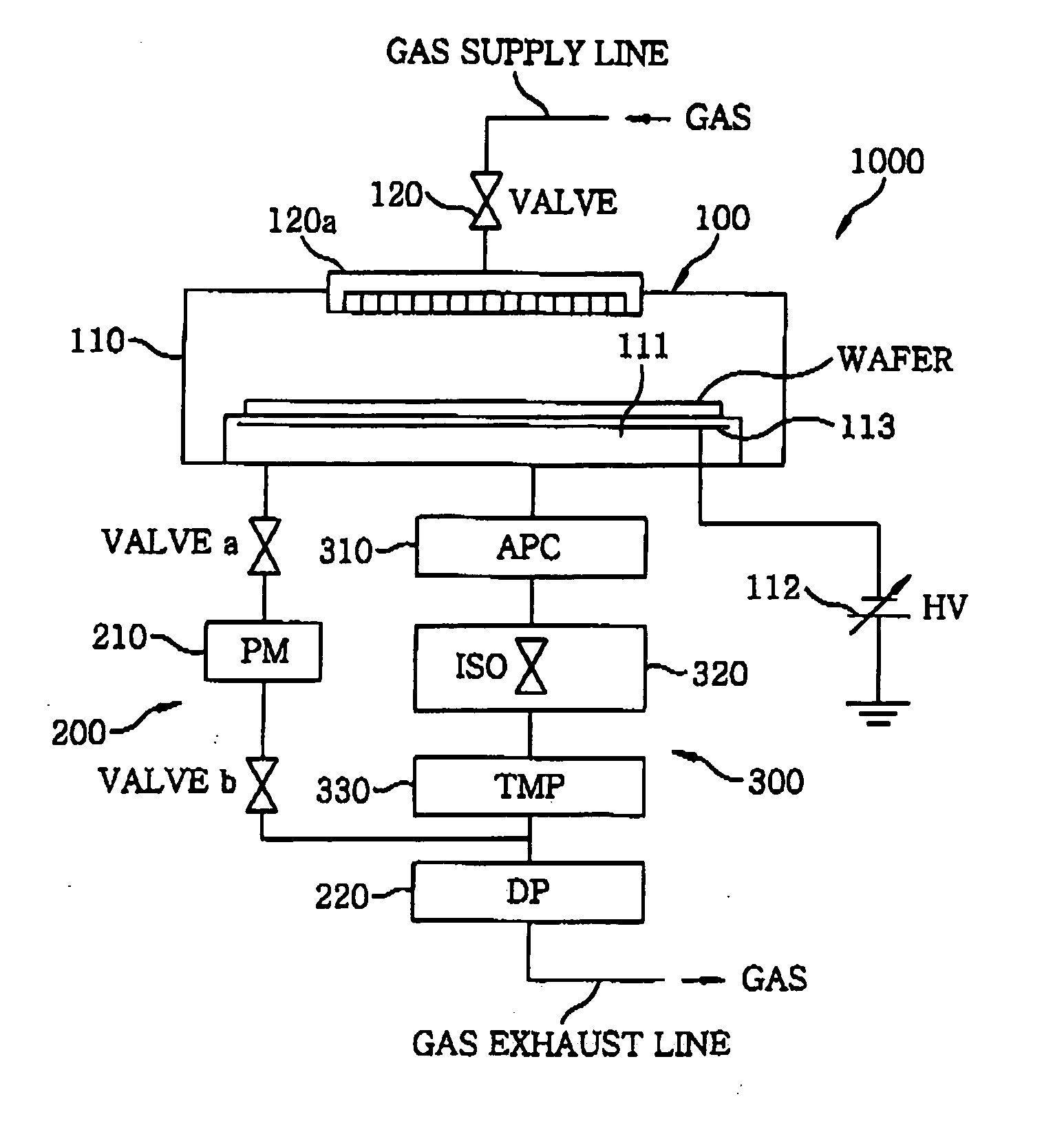
[0100] Though the first embodiment uses physical vibration generated by the supply of the purge gas, any type of vibration other than may also be used. For example, it is also preferable to apply ultrasonic waves of tens of kHz into the processing chamber 100 in order to generate vibration. Further, in case of utilizing the physical vibration, the gas supply line is preferred to have no orifice structure at a joint where it is connected with the processing chamber 100 or a vacuum transfer chamber 100′ to be describe later.

[0101] Moreover, it is preferable to generate physical vibration plural times. In such a case, since detachment of deposits reduces every time when the generation of physical vibration is repeated, the number of particles detected tends to be reduced. Thus, it is possible to perform a next manufacturing processing after the cleanness of the processing chamber 100 is evaluated as high.

[0102] The above first embodiment is preferably performed combined with the secon...

second embodiment

[0104] A semiconductor manufacturing apparatus 1000 in accordance with the second embodiment intermittently applies a high voltage HV to an electrode 113, for example, three times from a high voltage power supply 112. The applied high voltages HV are preferably not smaller than +1 kV or not greater than −1 kV. More preferably, a voltage of +1 kV and a voltage of −1 kV are applied alternately. As a result of applying the high voltages in this manner, an electromagnetic stress to be described below can be generated efficiently.

[0105] Whenever the high voltage HV is applied, a direct current (DC) discharge occurs instantaneously within the processing chamber 100, whereby a momentary potential gradient is formed on the chamber wall 110 or the wafer stage 111, thus creating an electromagnetic stress. Due to thus created electromagnetic stress, deposits on the chamber wall 110 or the wafer stage 111 are detached therefrom, and the detached deposits are discharged as particles along with t...

third embodiment

[0119] Moreover, though the vacuum transfer chamber 1000′ has been described to have the single exhaust line in the third embodiment, but it may have multiple exhaust lines. In case of multiple exhaust lines, though the multiple exhaust lines have normally different conductances (the conductance represents a coefficient indicating the fluidity of a fluid such as a discharged gas), any exhaust line of any conductance may employ this embodiment.

[0120] Further, it is preferable to combine the third embodiment with the second embodiment. In this case, a high voltage power supply identical to the high voltage power supply 112 is connected to the objects in the vacuum transfer chamber 100′.

[0121] In accordance with the first to the third embodiment descried above, though the cleanness of the processing chamber 100 or the vacuum transfer chamber 100′ is inspected under the absence of a wafer therein, it is also possible to evaluate the cleanness of an object other than the processing cham...


PUM

PropertyMeasurementUnit
thicknessaaaaaaaaaa
speedaaaaaaaaaa
diameteraaaaaaaaaa

Abstract

[Object]It is an object to provide a vacuum apparatus capable of evaluating its cleanness precisely by surely monitoring particles including deposits readily detached from the apparatus, and a particle monitoring method and program employed therein, and a window member for particle monitoring. [Constitution of the Invention]
A semiconductor manufacturing apparatus 1000 includes a processing chamber 100 for performing a manufacturing processing on a wafer. A gas supply line for introducing a purge gas is connected to an upper portion of the processing chamber 100, a valve 120 being installed on the gas supply line. A rough pumping line 200 with a valve a is connected to a lower portion of the processing chamber 100. Installed on the rough pumping line 200 are a dry pump 220 for exhausting a gas in the processing chamber 100 and a particle monitoring unit 210 for monitoring particles between the valve a and the dry pump 220. In the semiconductor manufacturing apparatus 1000, after the valve 120 is opened, the purge gas is supplied to apply physical vibration due to shock wave in the processing chamber 100 so that deposits are detached therefrom to be monitored as particles.

Description

FIELD OF THE INVENTION [0001] The present invention relates to a vacuum apparatus including a particle monitoring unit, a particle monitoring method and a program therefor, and a window member for use in the particle monitoring. BACKGROUND OF THE INVENTION [0002] A semiconductor manufacturing apparatus (FIG. 10) using plasma is employed to perform, for example, an etching processing on a semiconductor wafer (hereinafter, referred to as “wafer”) in the course of manufacturing semiconductor products. If particles generated during a manufacturing processing adhere to product wafers, the wafers would be contaminated, resulting in reduction in yield. Thus, a high level of cleanness is required for the semiconductor manufacturing apparatus. [0003]FIG. 10 illustrates a schematic configuration view of a conventional semiconductor manufacturing apparatus 800. [0004] In FIG. 10, the semiconductor manufacturing apparatus 800 includes a processing chamber 810 formed of a cylindrical vessel for ...

Claims


Application Information

Patent Timeline
Patent Type & Authority Applications(United States)
IPC IPC(8): B08B5/04B08B9/08B08B13/00B32B17/06G01M99/00G01N15/02G01N15/06H01J37/32
CPCB08B9/08G01N15/0272G01N15/06Y10T428/30H01J37/32935Y10T428/315G01N2015/0693Y10T428/8305
Inventor MORIYA, TSUYOSHINAKAYAMA, HIROYUKI
Owner TOKYO ELECTRON LTD
Why Eureka
Try Eureka