Transparent conductive film

a technology of transparent conductive film and conductive laminate, which is applied in the direction of oxide conductors, non-metal conductors, instruments, etc., can solve the problems of insufficient improvement of environment resistance at high temperature and high humidity, inferior flexibility and processability of conductive glass, and inability to be used in some cases, so as to achieve the effect of improving scratch resistance and bending resistan

Active Publication Date: 2005-12-08
NITTO DENKO CORP
View PDF1 Cites 29 Cited by
  • Summary
  • Abstract
  • Description
  • Claims
  • Application Information

AI Technical Summary

Benefits of technology

[0011] The present inventors have made eager investigation to examine the problem. As a result, it has been found, in regard to obtaining a transparent conductive film that is transparent and improved in scratch resistance and bending resistance by forming a transparent SiOx thin film, especially a transparent SiO2 thin film, on one side of a transparent base film and a transparent conductive thin film comprising an indium-tin complex oxide on the transparent SiOx thin film that when the transparent SiOx thin film is formed by a dry thin film forming method (i.e., a dry process) such as a vacuum deposition method, a sputtering method and an ion plating method, the surface of the transparent SiOx thin film is roughened, which results in high surface resistance in the obtained conductive thin film in the wake of the roughness of the transparent SiOx thin film, compared with a film formation by a wet coating method (i.e., a wet process) such as a sol-gel method, so that a high surface resistivity suitable for use such as touch panels can be obtained.

Problems solved by technology

However, since glass is used as a base, the conductive glass is inferior in flexibility and processability and cannot be used in some cases according to uses.
However, these kinds of conductive thin films are great in the reflectance of light of the thin film surface, so that they are inferior in transparency, resistance to scratch and bending, and susceptible to scratch during use to thereby increase electric resistance or disconnection of wires, and also inferior in environment resistance at high temperature and high humidity.
However, the improvement of environment resistance at high temperature and high humidity is still insufficient with the transparent conductive laminate.
However, when the film thickness is increased, the surface resistance of the transparent conductive laminate lowers, so that a surface resistivity suitable for a touch panel cannot be obtained.

Method used


Image

  • Transparent conductive film
  • Transparent conductive film

Examples


example 1

Production of Transparent Conductive Film

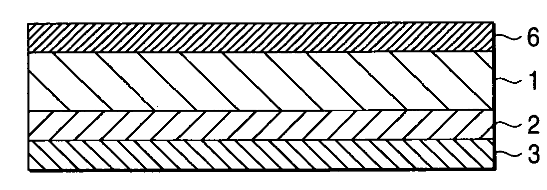
[0051] On one side of a transparent base film of a polyethylene terephthalate (hereinafter referred to as “PET”) film having a thickness of 25 μm, an SiOx (x=2.0) thin film having a thickness of 30 nm and a refractive index of light of 1.46 was formed by a vacuum deposition method. The average surface roughness of the SiOx thin film was 2.0 nm.

[0052] In the next place, a transparent conductive thin film comprising an indium-tin complex oxide (hereinafter referred to as an ITO thin film) having a thickness of 25 nm and a refractive index of light of 2.00 was formed on the SiOx thin film by using a sintered material including 95 wt % of indium oxide (In2O3) and 5 wt % of tin oxide (SnO2) in the atmosphere of 80% of argon gas and 20% of oxygen gas at 4×10⁻³ Torr by a reactive sputtering method, thereby a transparent conductive film was obtained.

Production of Hard Coat-Treated Film

[0053] A solution obtained by adding 5 parts of hydroxy-cycloh...

example 2

[0056] A transparent conductive film was manufactured in the same manner as in Example 1 except that the thickness of the ITO thin film was changed to 30 nm. A transparent conductive laminated film and a touch panel were manufactured with the transparent conductive film in the same manner as in Example 1.

example 3

[0057] A transparent conductive film was manufactured in the same manner as in Example 1 except that a sintered material including 90 wt % of indium oxide and 10 wt % of tin oxide was used. A transparent conductive laminated film and a touch panel were manufactured with the transparent conductive film in the same manner as in Example 1.


PUM

PropertyMeasurementUnit
surface roughnessaaaaaaaaaa
thicknessaaaaaaaaaa
refractive indexaaaaaaaaaa

Abstract

The present invention provides a transparent conductive film having: a transparent base film; a transparent SiOx thin film having a thickness of from 10 to 100 nm, a refractive index of from 1.40 to 1.80 and an average surface roughness Ra of from 0.8 to 3.0 nm, wherein x is from 1.0 to 2.0; and a transparent conductive thin film including an indium-tin complex oxide, which has a thickness of from 20 to 35 nm and a ratio of SnO2/(In2O3+SnO2) of from 3 to 15 wt %, wherein the transparent conductive thin film is disposed on one side of the transparent base film through the transparent SiOx thin film.

Description

FIELD OF THE INVENTION [0001] The present invention relates to a transparent conductive film having a transparent base film for use in a touch panel, a method for producing the transparent conductive film and a touch panel having the transparent conductive film. BACKGROUND OF THE INVENTION [0002] Thin films transparent for a light in the visible light region and having electric conductivity are generally used in display systems, e.g., a liquid crystal display and an electroluminescence display, transparent electrodes, e.g., a touch panel, and for the static prevention and cutoff of electromagnetic waves of transparent articles. As such a transparent conductive thin film, so-called conductive glass comprising a glass plate having formed thereon an indium oxide thin film is conventionally used. However, since glass is used as a base, the conductive glass is inferior in flexibility and processability and cannot be used in some cases according to uses. [0003] Therefore, in recent years,...

Claims


Application Information

Patent Timeline
Patent Type & Authority Applications(United States)
IPC IPC(8): G06F3/045H01B1/08H01L21/4763H01L23/48
CPCH01B1/08G06F3/045G02F1/1333
Inventor NASHIKI, TOMOTAKESUGAWARA, HIDEO
Owner NITTO DENKO CORP
Why Eureka
Try Eureka