Lithographic apparatus and device manufacturing method

a technology of lithographic apparatus and manufacturing method, which is applied in the direction of electrical apparatus, printers, instruments, etc., can solve the problems of limited compensation and conventional compensation methods, and achieve the effect of avoiding consequential reduction in throughpu

Active Publication Date: 2005-12-08
ASML NETHERLANDS BV
View PDF24 Cites 34 Cited by
  • Summary
  • Abstract
  • Description
  • Claims
  • Application Information

AI Technical Summary

Benefits of technology

[0029] In contrast, according to this embodiment of the present invention, doses up to the predetermined normal maximum for normal printing are used, but the method reserves at least one increased dose for compensation purposes. This can allow for that nominal white pixels in the projected radiation pattern to be used for compensation purposes. Thus, even when a dead black pixel falls in the middle of a group of surrounding white pixels it can be compensated, in the same exposure step, by increasing the radiation dose delivered by one or more of those neighboring white pixels, above the normal fully white value. This may conveniently be achieved by reserving one or more of the elements' most intense states (i.e., the states in which they interact with the projected beam to make the greatest contributions to their pixel's intensities) only for compensation purposes, the lower intensity states being used for normal printing.
[0031] In general, in a multi-step method, as much compensation as possible is made in each step for the effects of defective elements in that step using adjacent pixels. This reduces the amount of compensation to be provided by the other step or steps.
[0033] Compared with conventional methods, if the above embodiment produces the same final radiation dosage pattern on a substrate in the same time with the same number of passes / exposure steps, then it may employ an illumination system that delivers a more intense beam. The increased intensity is required to provide the capacity to deliver the radiation doses above the normal printing maximum. Although there are consequential increases in cost, significant improvements to the pattern quality are achieved as a result of the ability to compensate with white pixels, and a further advantage is the avoidance of an additional clean-up pass, which would reduce throughput.
[0045] Although a method embodying the invention may be carried out using elements which have a single black state, a single grey state, and a single white state, each non-defective element can also be controllable to selectively adopt one of a series of grey states and a series of white states, each grey or white state corresponding to a respective contribution to a corresponding pixel's peak intensity. The grey and white states may form a discrete or a continuous series. Preferably, each non-defective element may be controllable to adopt as many as 64 states, or more, to enable greyscale printing to be achieved. Hence, independence between the position of the projected radiation pattern and the “grid” defined by the array of controllable elements may be achieved.
[0051] The above embodiments can allow for better CD (charge dosage) control than with uncorrected dead pixels or than with conventional correction methods using surrounding pixels limited to 100% normal whiteness only.
[0053] Another embodiment can prevent a third pass being needed to print a missed dose in a clean-up scheme, and hence avoid the consequential reduction in throughput when using the same number of controllable element arrays (33%) or the additional cost for the element arrays, associated electronics, and wider projector field that would result if an additional element row were needed to provide clean-up doses.

Problems solved by technology

As discussed above, conventional compensation methods were limited to using compensation doses up to the normal printing maximum, i.e., the dose provided by a fully-white, non-defective pixel in a single exposure step / write pass.
Thus, compensation was limited to increasing the dose delivered by selected pixels in the projected pattern that would otherwise have been black or grey.

Method used


Image

  • Lithographic apparatus and device manufacturing method
  • Lithographic apparatus and device manufacturing method
  • Lithographic apparatus and device manufacturing method

Examples


Embodiment Construction

Overview and Terminology

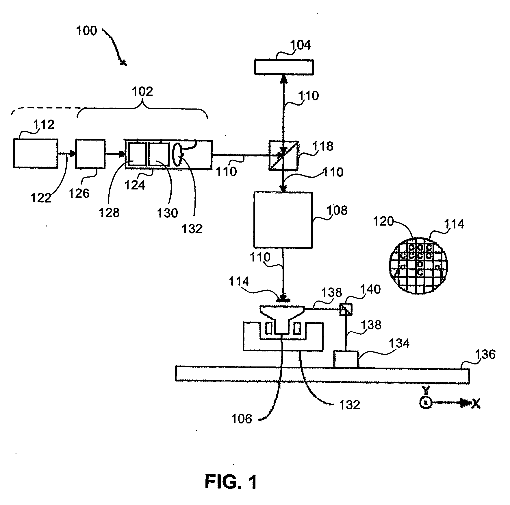
[0065] In one embodiment of the present invention using a microlens array imaging system, it is the function of a field lens of a beam expander (which field lens may be formed from two or more separate lenses) in an illumination system to make a projection system telecentric by ensuring that all components of the light beam between the field lens and the microlens array are parallel and perpendicular to the microlens array. However, although light beams between the field lens and the microlens array may be substantially parallel, absolute parallelism may not be achievable.

[0066] Thus, given a degree of non-telecentricity in the projection system, according to one embodiment of the present invention, small magnification adjustments can be achieved without undue loss of focus by displacing one or more of the lens components which are located between the pupil and the substrate table.

[0067] In one embodiment, a projection system will define a pupil. The term...


PUM

PropertyMeasurementUnit
wavelengthaaaaaaaaaa

Abstract

A system and method to manufacturing a device provide a substrate and perform at least one exposure step. Each exposure step projects a patterned beam of radiation, which was patterned using an individually controllable elements, onto a target portion of the substrate. The projected patterned beam includes a plurality of pixels. Each exposure step also: (a) ordinarily controls the elements, such that each pixel delivers a radiation dose no greater than a predetermined normal maximum dose to the target portion in the exposure step; and (b) exceptionally controls the elements, such that at least one selected pixel delivers an increased radiation dose, greater than the normal maximum dose. The increased dose may be delivered to compensate for the effect of a defective element at a known position in the array on a pixel adjacent a selected pixel. Alternatively, it may compensate for underexposure of the target portion at the location of a selected pixel resulting from exposure of that location to a pixel affected by a known defective element in another exposure step. The invention uses doses up to the predetermined normal maximum for normal printing, but reserves at least one increased dose for compensation purposes. Accordingly, even when a dead black pixel falls in the middle of a group of surrounding white pixels it can be compensated for by increasing the radiation dose delivered by one or more of those neighboring white pixels, above the normal fully white value.

Description

BACKGROUND OF THE INVENTION [0001] 1. Field of the Invention [0002] The present invention relates to a lithographic apparatus and a device manufacturing method. [0003] 2. Related Art [0004] A lithographic apparatus is a machine that applies a desired pattern onto a target portion of a substrate. The lithographic apparatus can be used, for example, in the manufacture of integrated circuits (ICs), flat panel displays, and other devices involving fine structures. In a conventional lithographic apparatus, a patterning means, which is alternatively referred to as a mask or a reticle, may be used to generate a circuit pattern corresponding to an individual layer of the IC (or other device), and this pattern can be imaged onto a target portion (e.g., comprising part of one or several dies) on a substrate (e.g., a silicon wafer or glass plate) that has a layer of radiation-sensitive material (e.g., resist). Instead of a mask, the patterning means may comprise an array of individually contro...

Claims


Application Information

Patent Timeline
Patent Type & Authority Applications(United States)
IPC IPC(8): G03F7/20G02B26/08H01L21/027
CPCG03F7/70275G03F7/70291G03F7/70058G03F7/70425G03F7/70383G03F7/7055
Inventor TROOST, KARS ZEGERBLEEKER, ARNO JAN
Owner ASML NETHERLANDS BV
Why Eureka
Try Eureka