

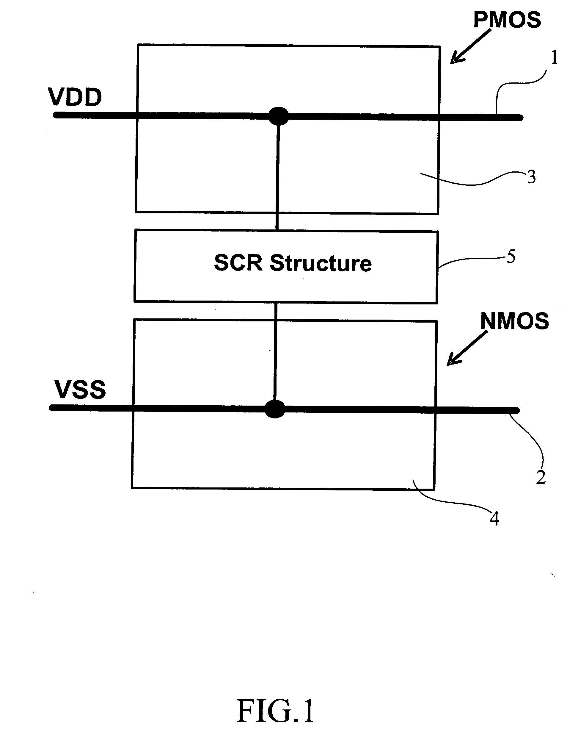
Silicon controlled rectifier for the electrostatic discharge protection
a technology of electrostatic discharge and rectifier, which is applied in the direction of circuit arrangements, semiconductor devices, transistors, etc., can solve the problems of ic function failure or even destruction, prone to latch-up issues of scr devices, etc., and achieve the effect of reducing layout area and improving robustness of the whole chip
- Summary
- Abstract
- Description
- Claims
- Application Information
AI Technical Summary
Benefits of technology
Problems solved by technology
Method used
Image

Examples
first embodiment
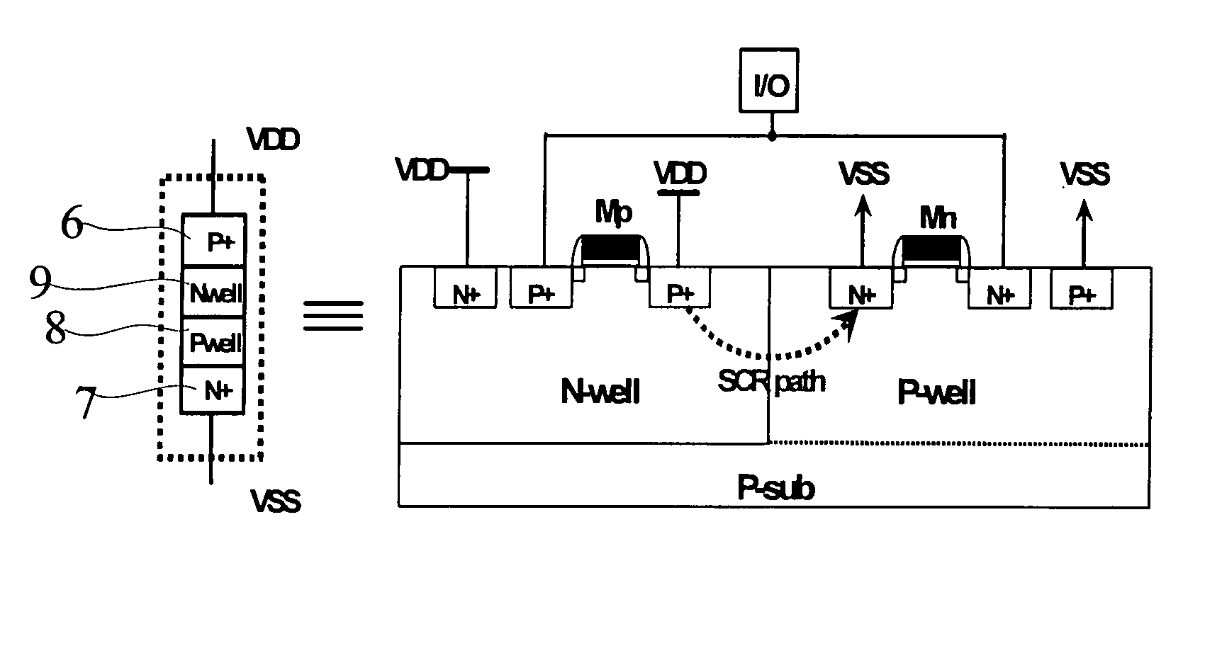
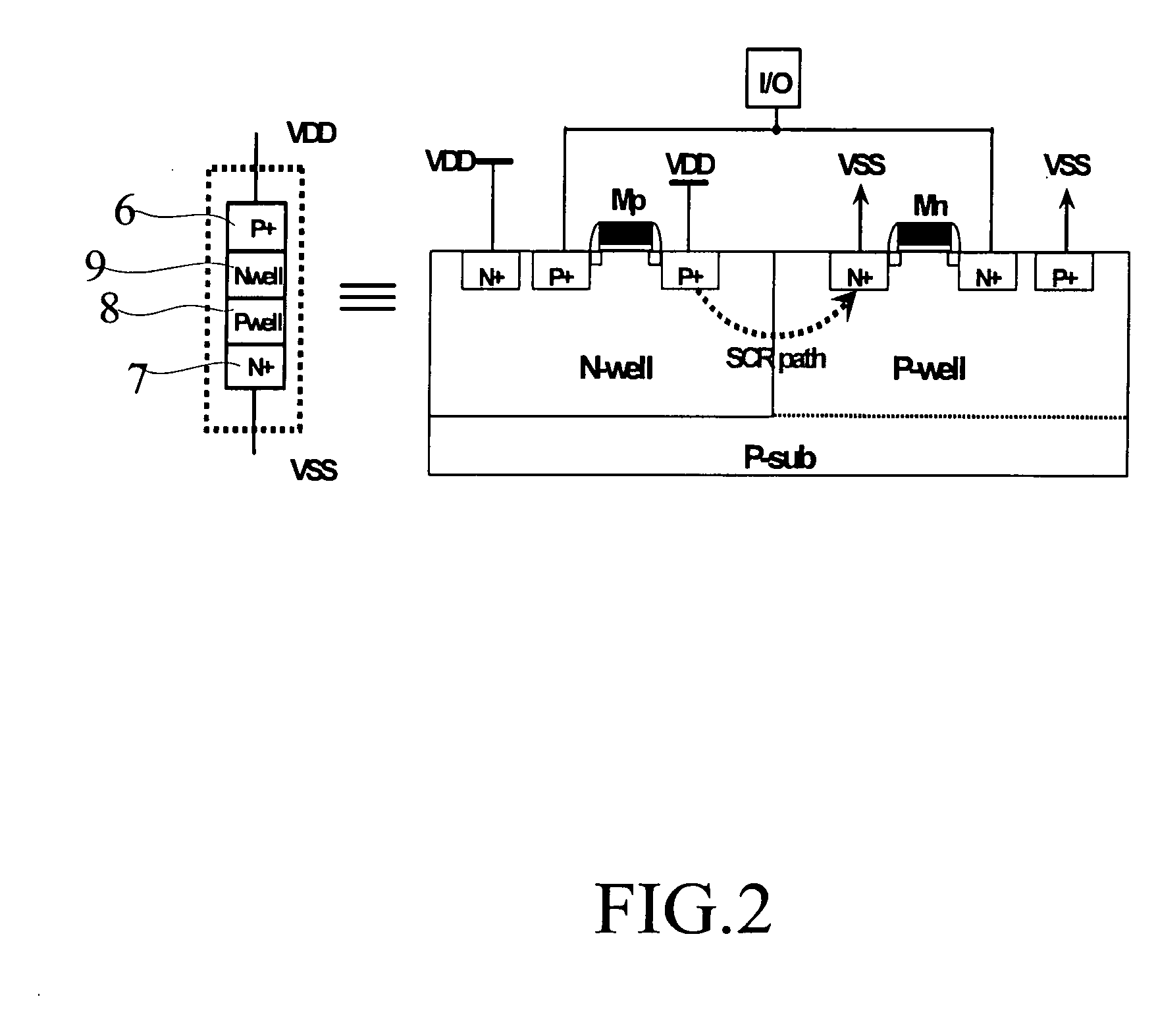
[0057] Please refer to FIG. 2. The SCR structure 5 of the present invention is comprised of a first P-typed high-doped region (P+) 6, a first N-typed high-doped region (N+) 7, a P-well 8 and an N-well 9. Additionally, the SCR structure 5 can be collocated with FIG. 16 to protect internal circuit, wherein FIG. 16 is a view showing circuit according to the present invention.
[0058] Please refer to FIG. 3. The SCR structure 5 of the present invention is comprised of a first P-typed high-doped region (P+) 6, a first N-typed high-doped region (N+) 7, a P-well 8 and an N-well 9, and is further comprised of a second P-typed high-doped region (P+) 10 as an anode and a second N-typed high-doped region (N+) 11 as a cathode. Additionally, the SCR structure 5 can be collocated with FIG. 16 to protect internal circuit, wherein FIG. 16 is a view showing a first embodiment of circuit according to the present invention.
second embodiment
[0059] Please refer to FIG. 4. The SCR structure 5 of the present invention is comprised of a first P-typed high-doped region (P+) 6, a first N-typed high-doped region (N+) 7, a P-well 8, an N-well 9 and a third P-typed high-doped region (P+) 12. Additionally, the SCR structure 5 can be collocated with FIG. 17 to protect internal circuit, wherein FIG. 17 is a view showing circuit according to the present invention.
third embodiment
[0060] Please refer to FIG. 5. The SCR structure 5 of the present invention is comprised of a first P-typed high-doped region (P+) 6, a first N-typed high-doped region (N+) 7, a P-well 8, an N-well 9 and a third N-typed high-doped region (N+) 13. Additionally, the SCR structure 5 can be collocated with FIG. 18 to protect internal circuit, wherein FIG. 18 is a view showing circuit according to the present invention.
[0061] Please refer to FIG. 6, the SCR structure 5 of the present invention is comprised of a first P-typed high-doped region (P+) 6, a first N-typed high-doped region (N+) 7, a P-well 8, an N-well 9, a second P-typed high-doped region (P+) 10 as an anode, a second N-typed high-doped region (N+) 11 as a cathode and a third P-typed high-doped region(P+) 12. Additionally, the SCR structure 5 can be collocated with FIG. 17 to protect internal circuit, wherein FIG. 17 is a view showing a second embodiment of circuit according to the present invention.
[0062] Please refer to FI...
PUM
 Abstract
Description
Claims
Application Information