Pre-doped reflow interconnections for copper pads

a technology of reflow interconnection and copper pads, which is applied in the direction of semiconductor/solid-state device details, soldering apparatus, manufacturing tools, etc., can solve the problem of reducing the interfacial strength of the intermetallic joint, and achieve the effect of reducing the diffusion rate of the first metal

Inactive Publication Date: 2005-12-15
TEXAS INSTR INC
View PDF8 Cites 69 Cited by
  • Summary
  • Abstract
  • Description
  • Claims
  • Application Information

AI Technical Summary

Benefits of technology

[0005] A need has arisen for a straightforward solution to improve the reliability of direct copper / solder contacts. A careful investigation has been conducted to study the interface between copper and solder under the long term influence of elevated temperatures or repeated temperature cycles, commonly referred to as “aging”. This investigation has confirmed that after aging a large amount of Kirkendall voids has formed at the interface between solder and copper, which greatly decreases the interfacial strength of the intermetallic joint.
[0009] Another embodiment of the present invention is a metal interconnect structure comprising a bond pad of a first metal and a body of reflow alloy in contact with the bond pad. The alloy includes a quantity of the first metal sufficient to reduce the diffusion rate of the first metal into the alloy, and to substantially prevent the formation of Kirkendall voids at the first metal / alloy body intermetallic joint, and concurrently to keep the alloy melting temperature less than about 20° C. above the eutectic temperature of the alloy. Finally, the structure has a contact pad comprising a third metal in contact with the alloy body.

Problems solved by technology

This investigation has confirmed that after aging a large amount of Kirkendall voids has formed at the interface between solder and copper, which greatly decreases the interfacial strength of the intermetallic joint.

Method used


Image

  • Pre-doped reflow interconnections for copper pads
  • Pre-doped reflow interconnections for copper pads

Examples


Embodiment Construction

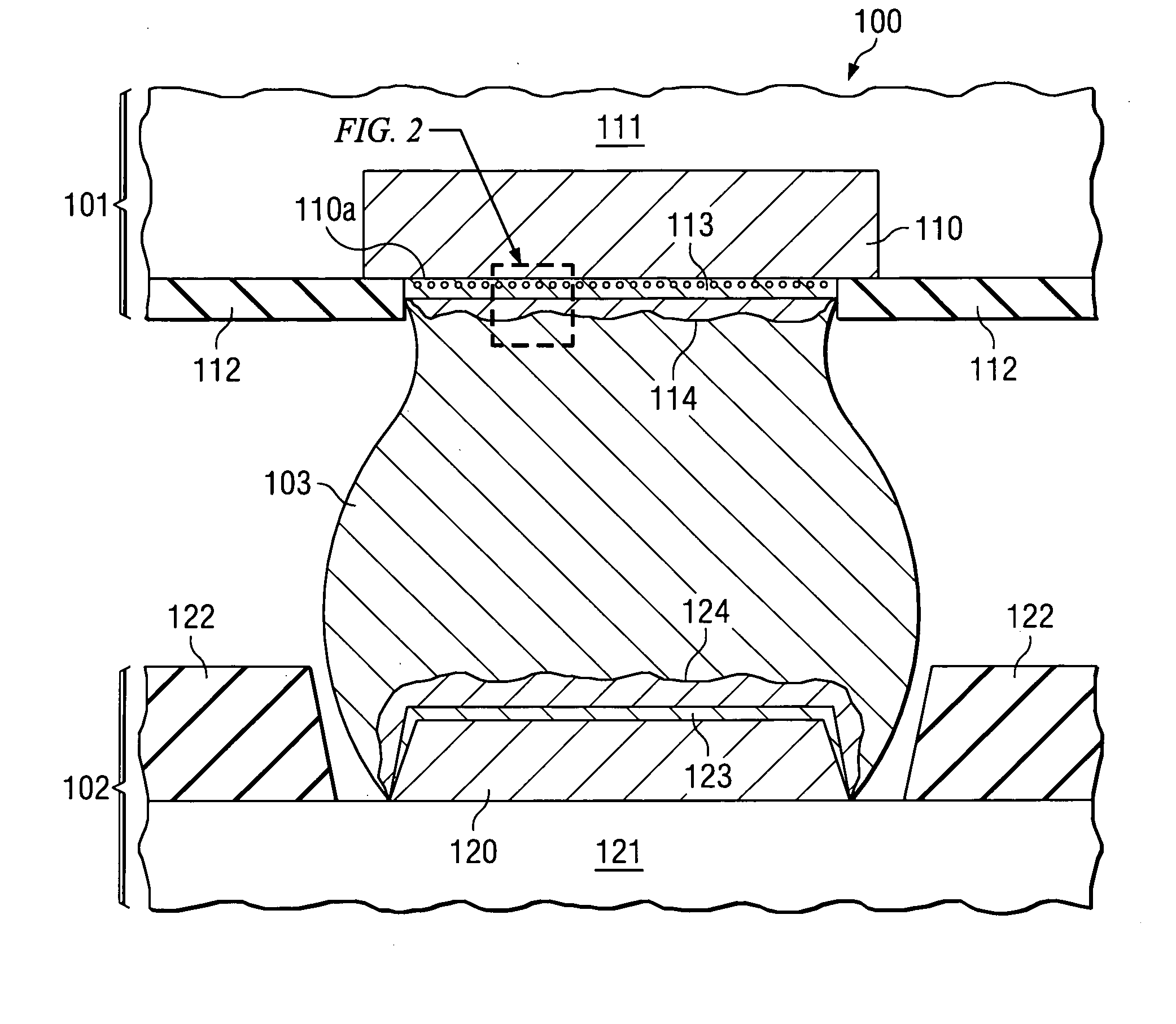
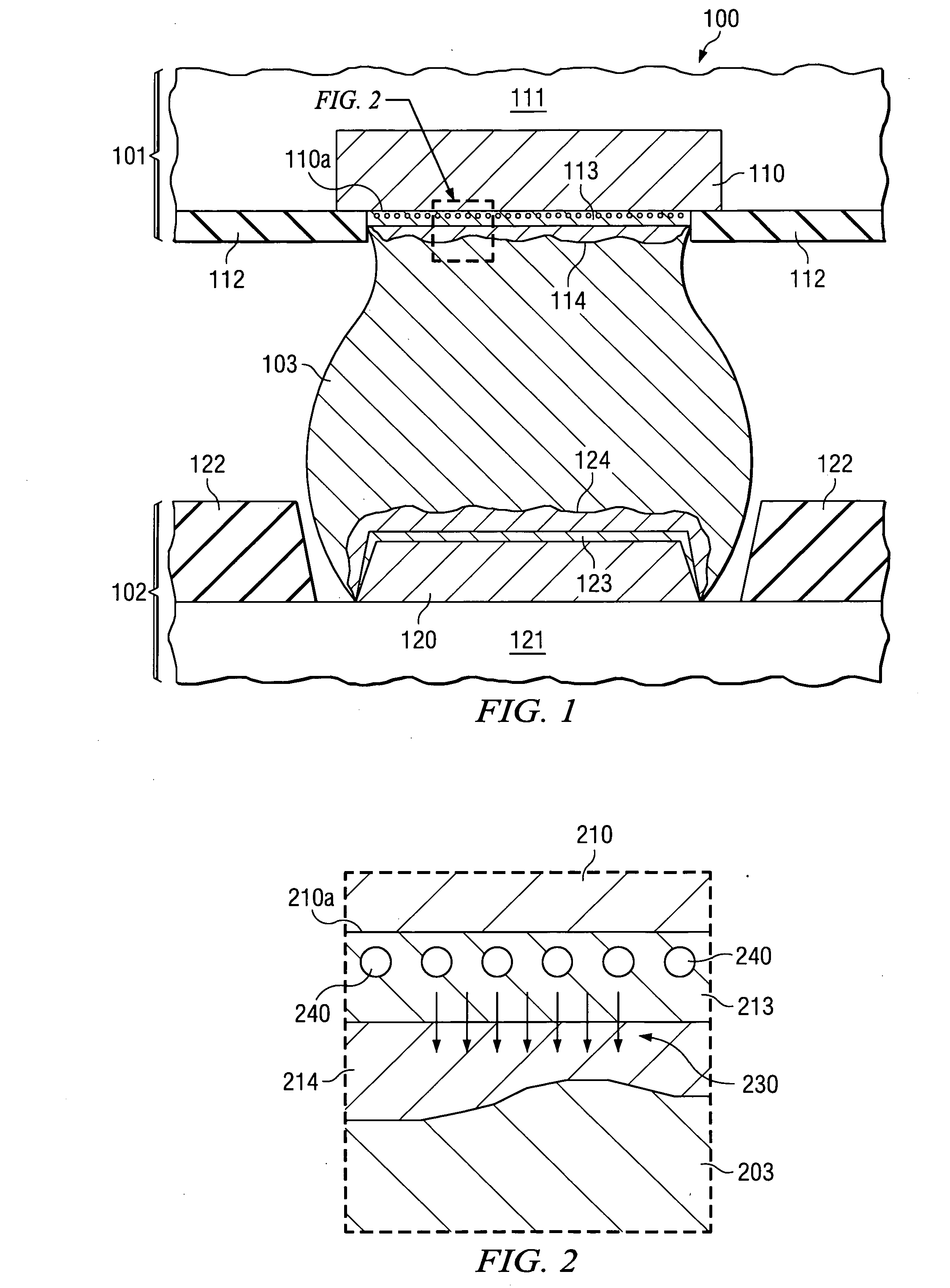
[0013] The present invention is related to U.S. patent application Ser. No. 10 / 434,316, filed on May 7, 2003 (Zeng, “Controlling Interdiffusion Rates in Metal Interconnection Structures”).

[0014] In the schematic cross section of FIG. 1, a portion of a product, generally designated 100, is shown comprising a device part designated 101, a substrate designated 102, and a means for attachment, designated 103, which attaches device 101 to substrate 102.

[0015] In the specific embodiments discussed here, device 101 is a semiconductor device. It may be a semiconductor chip, or it may be a semiconductor package. In either case, the device has a metallic bond pad 110, which is made of copper. In some embodiments, bond pad 110 comprises a copper alloy. Bond pad 110 is surrounded by insulating material 111; examples are silicon dioxide, silicon nitride, silicon carbide, low-k dielectrics, polymer compounds such as polyimides, glass ceramics, FR-4 and other composites. Part of the pad surface ...


PUM

PropertyMeasurementUnit
eutectic temperatureaaaaaaaaaa
temperaturesaaaaaaaaaa
dielectric constantaaaaaaaaaa

Abstract

A metal interconnect structure (100) comprising a bond pad (110) of copper; a body (103) of eutectic alloy in contact with the bond pad, this alloy including copper; and a contact pad (120) comprising copper in contact with the alloy body. When the eutectic alloy is tin / lead, the alloy includes copper in an amount greater than 0.08 weight percent and less than 2.0 weight percent. When the eutectic alloy is tin / silver, the alloy includes copper in an amount greater than 0.9 weight percent and less than 2.0 weight percent.

Description

FIELD OF THE INVENTION [0001] The present invention is related in general to the field of semiconductor devices and more specifically to a method of controlling metal interdiffusion and diminishing Kirkendall voids in interconnections, especially in solder joints, to improve device reliability. DESCRIPTION OF THE RELATED ART [0002] When integrated circuits on semiconductor chips are to be interconnected to external circuitry on a substrate using reflow materials such as solder, the parts to be assembled have to undergo at least one temperature rise to above the melting temperature of the reflow material, followed by a cooling cycle. After completing this process, the finished assembly often has to be subjected to annealing steps, consisting typically of repeated temperature swings for an extended period of time. Finally, the assembled parts frequently have to be tested to determine their reliable functioning after repeated exposure to failure-accelerating conditions such as extreme ...

Claims


Application Information

Patent Timeline
Patent Type & Authority Applications(United States)
IPC IPC(8): B23K35/26H01L23/485H01L23/52H05K3/34
CPCB23K35/262H01L24/02H01L24/10H01L2224/0401H01L2224/13023H01L2224/13099H01L2924/01006H01L2924/01014H01L2924/01028H01L2924/01029H01L2924/0103H01L2924/01047H01L2924/01049H01L2924/0105H01L2924/01075H01L2924/01078H01L2924/01079H01L2924/01082H01L2924/01322H01L2924/01327H01L2924/014H01L2924/05042H01L2924/09701H01L2924/14H05K3/3436H05K3/3463H01L2924/01019H01L2924/01033H01L2924/01087H01L24/13H01L2224/13H01L2924/00H01L2224/16503H01L2224/08503H01L2224/08505H01L24/03H01L24/05H01L24/16
Inventor ZENG, KEJUNCHIU, TZ-CHENGHOLDFORD, REBECCA L.
Owner TEXAS INSTR INC
Why Eureka
Try Eureka