Method for manufacturing a semiconductor device having polysilicon plugs

a semiconductor device and polysilicon technology, applied in the direction of semiconductor devices, basic electric elements, electrical appliances, etc., can solve the problems of increasing leakage current, conventional methods for manufacturing dram devices, and unable to achieve both junction leakage current reduction and contact resistance reduction in memory cells. , to achieve the effect of reducing contact resistan

Inactive Publication Date: 2005-12-22
LONGITUDE SEMICON S A R L
View PDF6 Cites 13 Cited by
  • Summary
  • Abstract
  • Description
  • Claims
  • Application Information

AI Technical Summary

Benefits of technology

[0016] In view of the above problems in the conventional techniques, it is an object of the present invention to provide a method for manufacturing a semiconductor device which is capable of suppressing a junction leakage current in a transistor and reducing the contact resistance between the contact plug and the diffused region of the transistor.

Problems solved by technology

This structure is not used in the memory cell area 10A however, because there is a possibility that junction leakage current is increased because the metallic atoms such as titanium and cobalt are diffused within the silicon substrate to form recombination centers.
However, conventional methods for manufacturing a DRAM device have respective drawbacks and cannot achieve both a reduced junction leakage current and a lower contact resistance in the memory cell.

Method used


Image

  • Method for manufacturing a semiconductor device having polysilicon plugs
  • Method for manufacturing a semiconductor device having polysilicon plugs
  • Method for manufacturing a semiconductor device having polysilicon plugs

Examples


Embodiment Construction

[0030] Before describing preferred embodiments of the present invention, the principle of the present invention will be described for a better understanding of the present invention. The present inventors found the causes of the junction leakage current by analyses and experiments as detailed below.

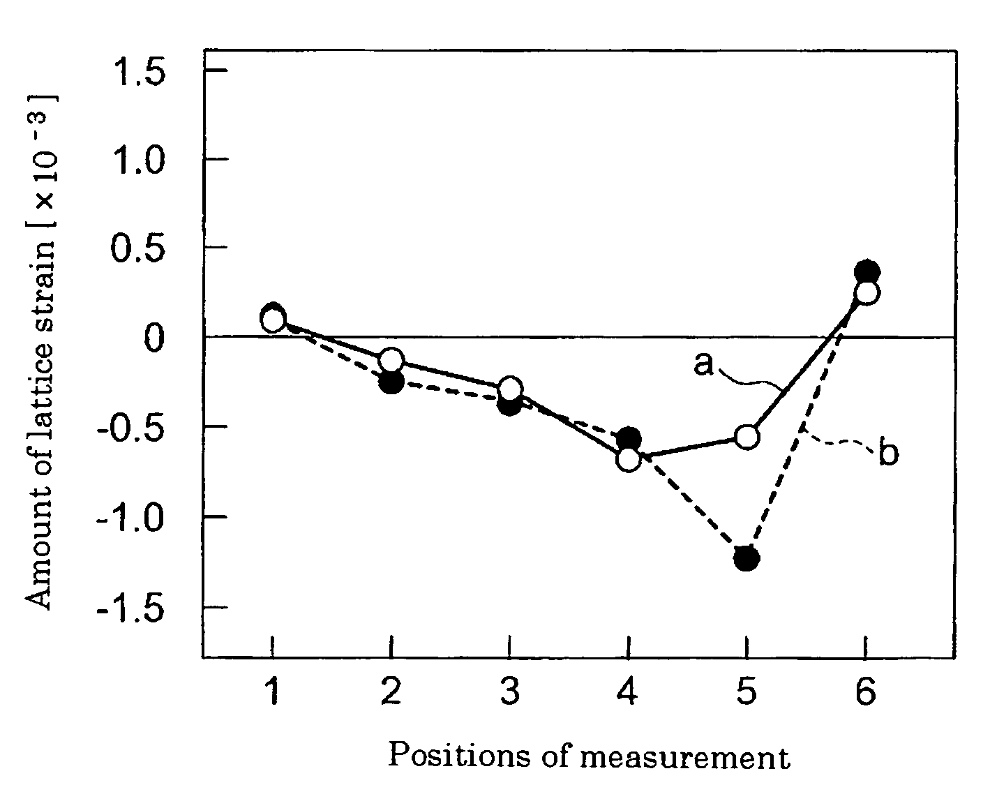
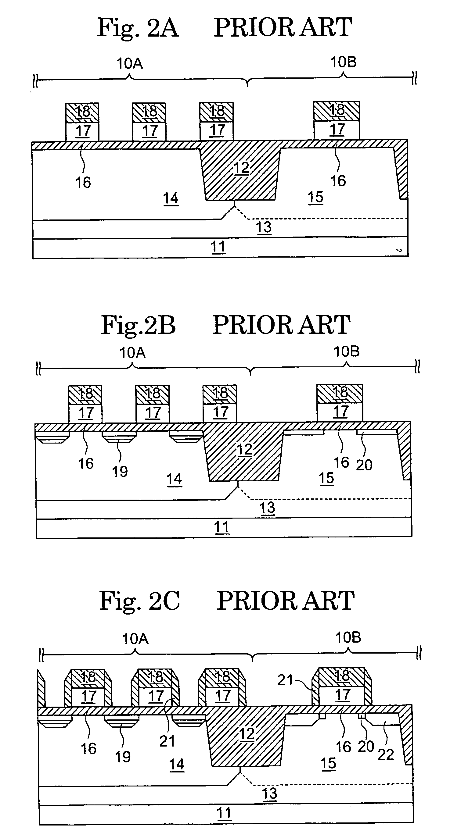
[0031] It is noted in the step shown in FIG. 2B that the phosphorous implantation into the memory cell area 10A expels silicon atoms from the lattices of the silicon crystal structure to generate vacancy-type defects and interstitial silicon atoms. The vacancy-type defect is such that a silicon atom is expelled from a lattice without substitute by another atom. Since the interstitial silicon atom has a higher diffusion rate compared to the vacancy-type defect, most interstitial silicon atoms are scattered during a heat treatment effected succeeding to the ion-implantation. This causes an excess of the number of vacancy-type defects in the vicinity of the n-type diffused region 19.

[0032]...


PUM


Abstract

A method for manufacturing a DRAM device on a silicon substrate includes: forming cell transistors in a memory cell area and other transistors in a peripheral circuit area; forming polysilicon plugs connected to diffused regions of the cell transistors and metallic plugs connected to diffused regions of the other transistors; heat treating at a temperature of 980 to 1,020 degrees C.; heat treating at a temperature of 700 to 850 degrees C.; implanting fluorine or boron fluoride into the diffused regions of the other transistors; and heat treating at a temperature of 500 to 850 degrees C.

Description

BACKGROUND OF THE INVENTION [0001] (a) Field of the Invention [0002] The present invention relates to a method for manufacturing a semiconductor device having polysilicon plugs and, more particularly, to a heat treatment technique after forming polysilicon plugs in a semiconductor device. [0003] (b) Description of the Related Art [0004] A DRAM (dynamic random access memory) device includes therein a memory cell area for storing data and a peripheral circuit area for controlling write / read of data into / from the memory cell area. Each DRAM memory cell in the memory cell area includes a capacitor for storing therein electric charge and a cell transistor acting as a switch for supplying the electric charge to the capacitor. A cell transistor may include a polysilicon electrode, or polysilicon plug, in contact with a diffused region of the cell transistor. [0005]FIGS. 2A to 2F consecutively show a conventional fabrication process for manufacturing a DRAM device. First, as shown in FIG. 2...

Claims


Application Information

Patent Timeline
Patent Type & Authority Applications(United States)
IPC IPC(8): H01L21/265H01L21/285H01L21/324H01L21/336H01L21/768H01L21/8242
CPCH01L21/26506H01L21/26513H01L21/28518H01L21/28525H01L21/324H01L29/66575H01L27/10855H01L27/10873H01L27/10888H01L27/10894H01L21/76877H10B12/05H10B12/485H10B12/0335H10B12/09H10B99/00
Inventor OKONOGI, KENSUKEOHYU, KIYONORIMANABE, KAZUTAKAYAMADA, SATORUOHASHI, TAKUO
Owner LONGITUDE SEMICON S A R L
Why Eureka
Try Eureka