Film formation apparatus and method for semiconductor process

a technology of film formation apparatus and semiconductor process, which is applied in the direction of chemistry apparatus and processes, crystal growth processes, coatings, etc., can solve the problems of low vapor pressure of doping gases of this kind, low consumption (outflow) per unit time of diluted doping gas from storage cylinders, and low uniform doping distribution, so as to improve the diffusion rate of doping gas, reduce the exchange frequency of doping gas sources, and improve the effect of productivity or throughpu

Inactive Publication Date: 2005-12-22
TOKYO ELECTRON LTD
View PDF7 Cites 36 Cited by
  • Summary
  • Abstract
  • Description
  • Claims
  • Application Information

AI Technical Summary

Benefits of technology

[0009] An object of the present invention is to increase the diffusion rate of a doping gas within a process container, while decreasing the exchange frequency of a doping gas source, thereby improving the productivity or throughput in a film formation apparatus and method for a semiconductor process.

Problems solved by technology

However, in general, doping gases of this kind have a very low vapor pressure.
Accordingly, where a doping gas in a pure state is supplied into a process container, it cannot diffuse sufficiently, thereby resulting in a less uniform doping distribution.
However, in this case, as described above, the consumption (outflow) per unit time of the diluted doping gas from the storage cylinder is very high.
As a consequence, the storage cylinder needs to be replaced with a new one in a relatively short time, thereby resulting in a low productivity and thus a low throughput.

Method used


Image

  • Film formation apparatus and method for semiconductor process
  • Film formation apparatus and method for semiconductor process
  • Film formation apparatus and method for semiconductor process

Examples


Embodiment Construction

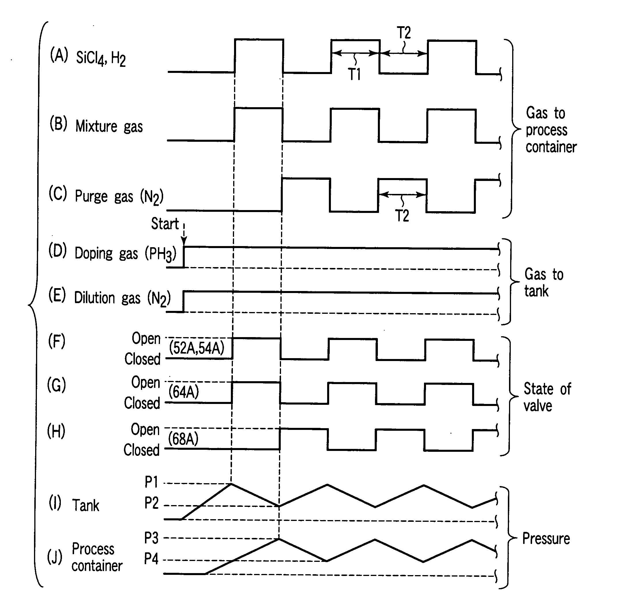
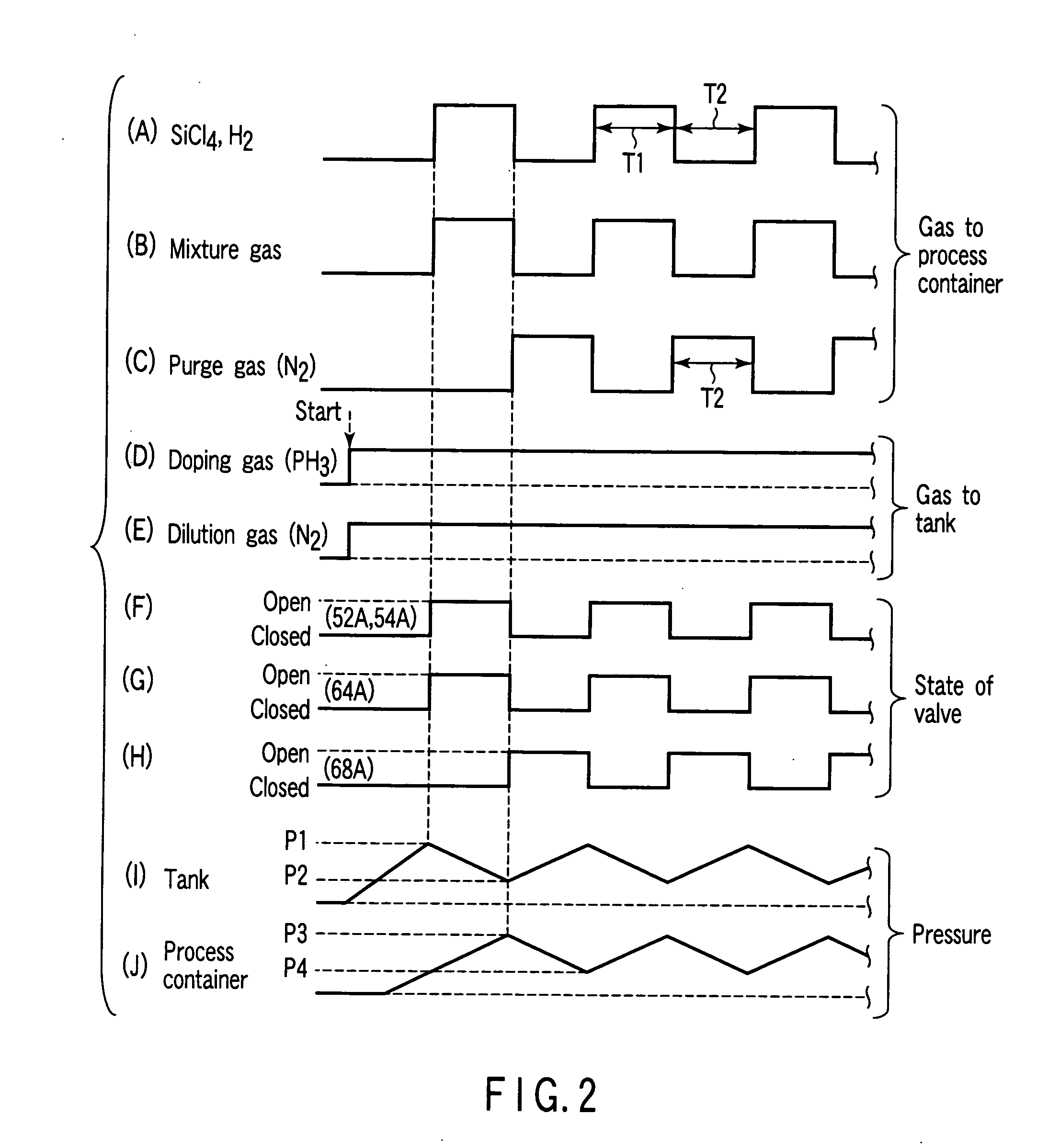
[0034] An embodiment of the present invention will now be described with reference to the accompanying drawings. In the following description, the constituent elements having substantially the same function and arrangement are denoted by the same reference numerals, and a repetitive description will be made only when necessary.

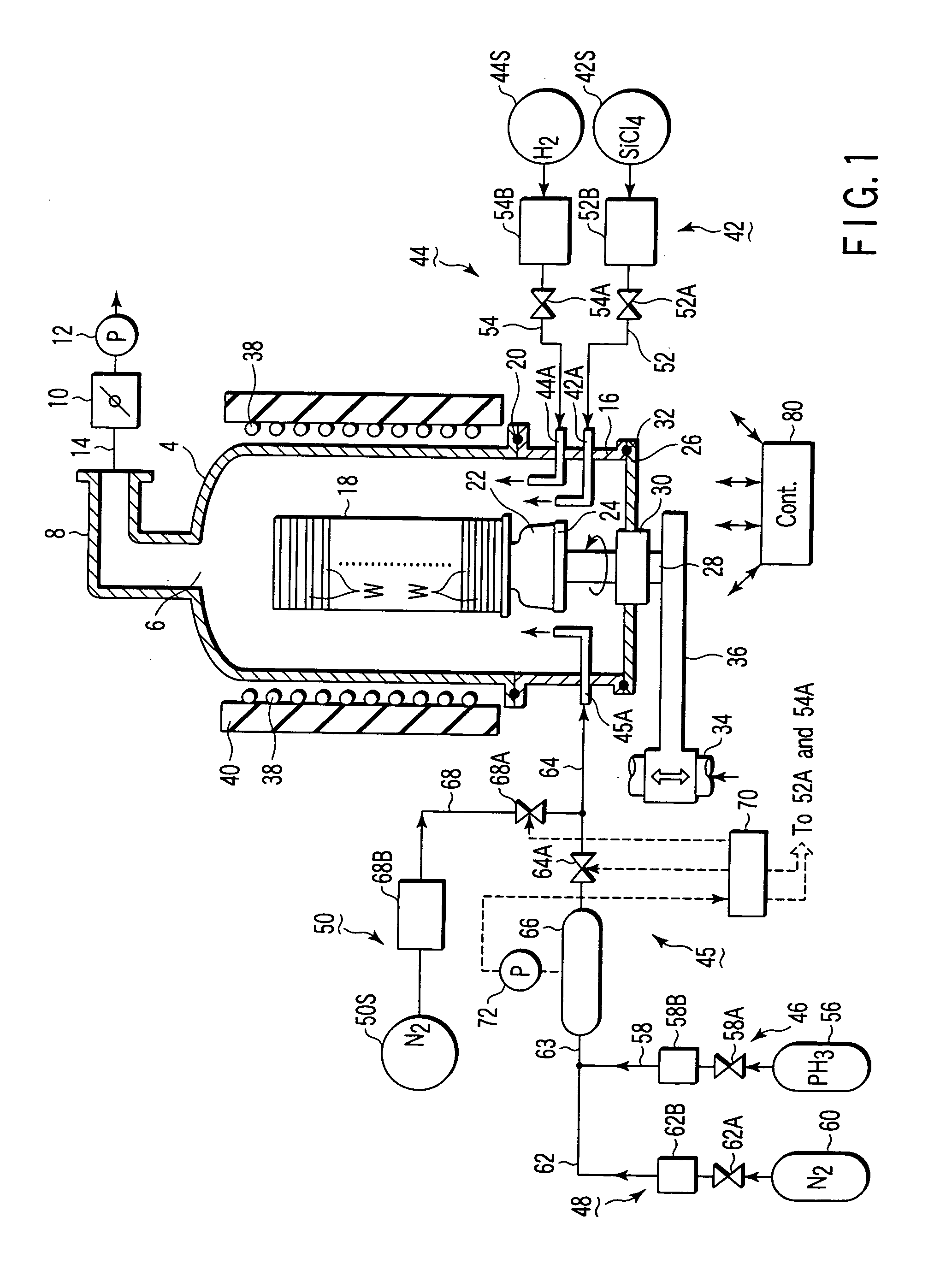
[0035]FIG. 1 is a structural view showing a vertical film formation apparatus (CVD apparatus) according to an embodiment of the present invention. As shown in FIG. 1, the film formation apparatus 2 includes a vertical process container 4, which is cylindrical and opened at the bottom. The process container 4 is made of, e.g., quartz, which is high in heat resistance. An exhaust port 6 is formed at the top of the process container 4. The exhaust port 6 is connected to, e.g., an exhaust nozzle 8 laterally bent at right angles. The exhaust nozzle 8 is connected to an exhaust system 14 including a pressure control valve 10 and a vacuum pump 12, provided thereon. ...


PUM

PropertyMeasurementUnit
volumeaaaaaaaaaa
sizeaaaaaaaaaa
diameteraaaaaaaaaa

Abstract

A film formation apparatus for a semiconductor process includes a source gas supply circuit to supply into a process container a source gas for depositing a thin film on target substrates, and a mixture gas supply circuit to supply into the process container a mixture gas containing a doping gas for doping the thin film with an impurity and a dilution gas for diluting the doping gas. The mixture gas supply circuit includes a gas mixture tank disposed outside the process container to mix the doping gas with the dilution gas to form the mixture gas, a mixture gas supply line to supply the mixture gas from the gas mixture tank into the process container, a doping gas supply circuit to supply the doping gas into the gas mixture tank, and a dilution gas supply circuit to supply the dilution gas into the gas mixture tank.

Description

CROSS-REFERENCE TO RELATED APPLICATIONS [0001] This application is based upon and claims the benefit of priority from prior Japanese Patent Applications No. 2004-182361, filed Jun. 21, 2004; and No. 2005-141401, filed May 13, 2005, the entire contents of both of which are incorporated herein by reference. BACKGROUND OF THE INVENTION [0002] 1. Field of the Invention [0003] The present invention relates to a film formation apparatus and method for a semiconductor process for forming a thin film doped with an impurity (dopant), such as phosphorous (P) or boron (B), on a target substrate, such as a semiconductor wafer. The term “semiconductor process” used herein includes various kinds of processes which are performed to manufacture a semiconductor device or a structure having wiring layers, electrodes, and the like to be connected to a semiconductor device, on a target substrate, such as a semiconductor wafer or a glass substrate used for an LCD (Liquid Crystal Display) or FPD (Flat Pa...

Claims


Application Information

Patent Timeline
Patent Type & Authority Applications(United States)
IPC IPC(8): C23C16/00C23C16/24H01L21/26H01L21/42
CPCC23C16/24Y10T117/1024C23C16/45523H01L21/205H01L21/285
Inventor HASEBE, KAZUHIDECHOU, PAO-HWAKIM, CHAEHO
Owner TOKYO ELECTRON LTD
Why Eureka
Try Eureka