Micro-etching method to replicate alignment marks for semiconductor wafer photolithography

a technology of alignment marks and micro-etching, which is applied in the direction of semiconductor devices, semiconductor/solid-state device details, electrical devices, etc., can solve the problems of insufficient accuracy of manual assisted method for blind positioning process wafers for alignment mark etching, insufficient accuracy of conventional method for forming and replicating alignment marks, and increasing difficulty in forming feature patterns overlying previously defined semiconductor device levels

Inactive Publication Date: 2005-12-22
TAIWAN SEMICON MFG CO LTD
View PDF3 Cites 13 Cited by
  • Summary
  • Abstract
  • Description
  • Claims
  • Application Information

AI Technical Summary

Problems solved by technology

With the high integration of the semiconductor devices, the accuracy of formation of feature patterns overlying a previously defined semiconductor device level is increasingly difficult as critical dimensions shrink.
As device technologies scale to about 0.10 microns and below, conventional method for forming and replicating alignment marks are no longer sufficiently accurate.
One problem according to prior art methods of replicating alignment marks, is that the manually assisted method for blindly positioning the process wafer for alignment mark etching is not sufficiently accurate, frequently requiring the formation of a relatively wide clear out window surrounding the alignment mark areas to ensure exposure of the alignment marks during etching.
Further, the need for an additional photolithographic patterning and etching process to clear out the alignment mark areas significantly increases the processing time.
Other shortcomings in the prior art methods for replicating alignment mark areas include the possibility of overpolishing the alignment mark area during the STI oxide CMP process, thereby reducing a thickness window of the underlying silicon nitride layer and leading to the potentiality of damage to the silicon substrate.
Another problem in prior art method for replicating alignment marks is the relative contrast of the alignment marks which are detected by an auto-imaging system.
As overlay budgets approach 20 to 30 nanometers for 0.10 micron critical dimensions and lower, a small decrease in the definition of the alignment marks by overlayers of high extinction coefficient materials is increasingly detrimental to overlay accuracy.
In many cases an additional step to photolithographically pattern and etch the alignment mark area is economically prohibitive in terms of process cycle time and material cost.

Method used


Image

  • Micro-etching method to replicate alignment marks for semiconductor wafer photolithography
  • Micro-etching method to replicate alignment marks for semiconductor wafer photolithography
  • Micro-etching method to replicate alignment marks for semiconductor wafer photolithography

Examples


Embodiment Construction

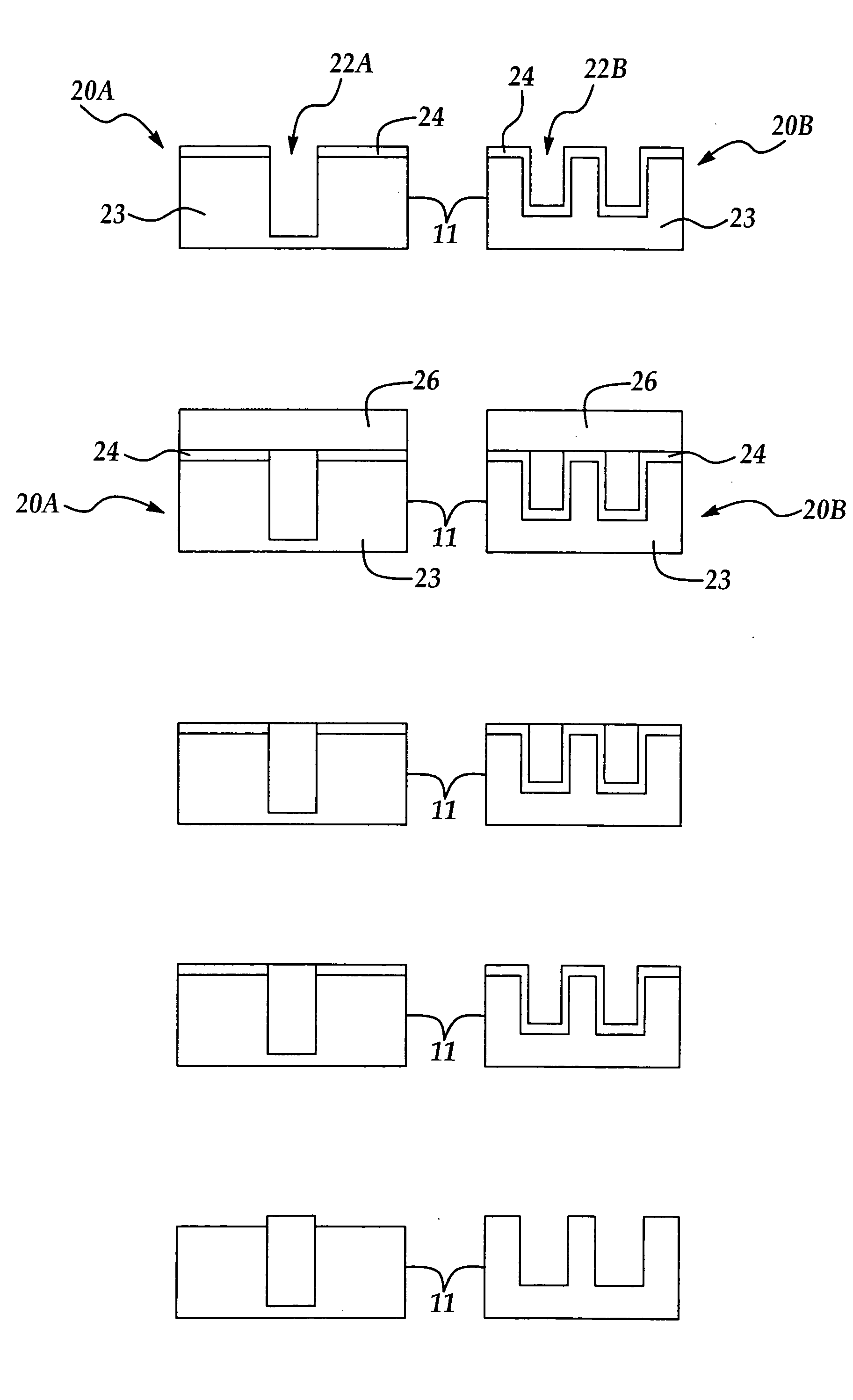
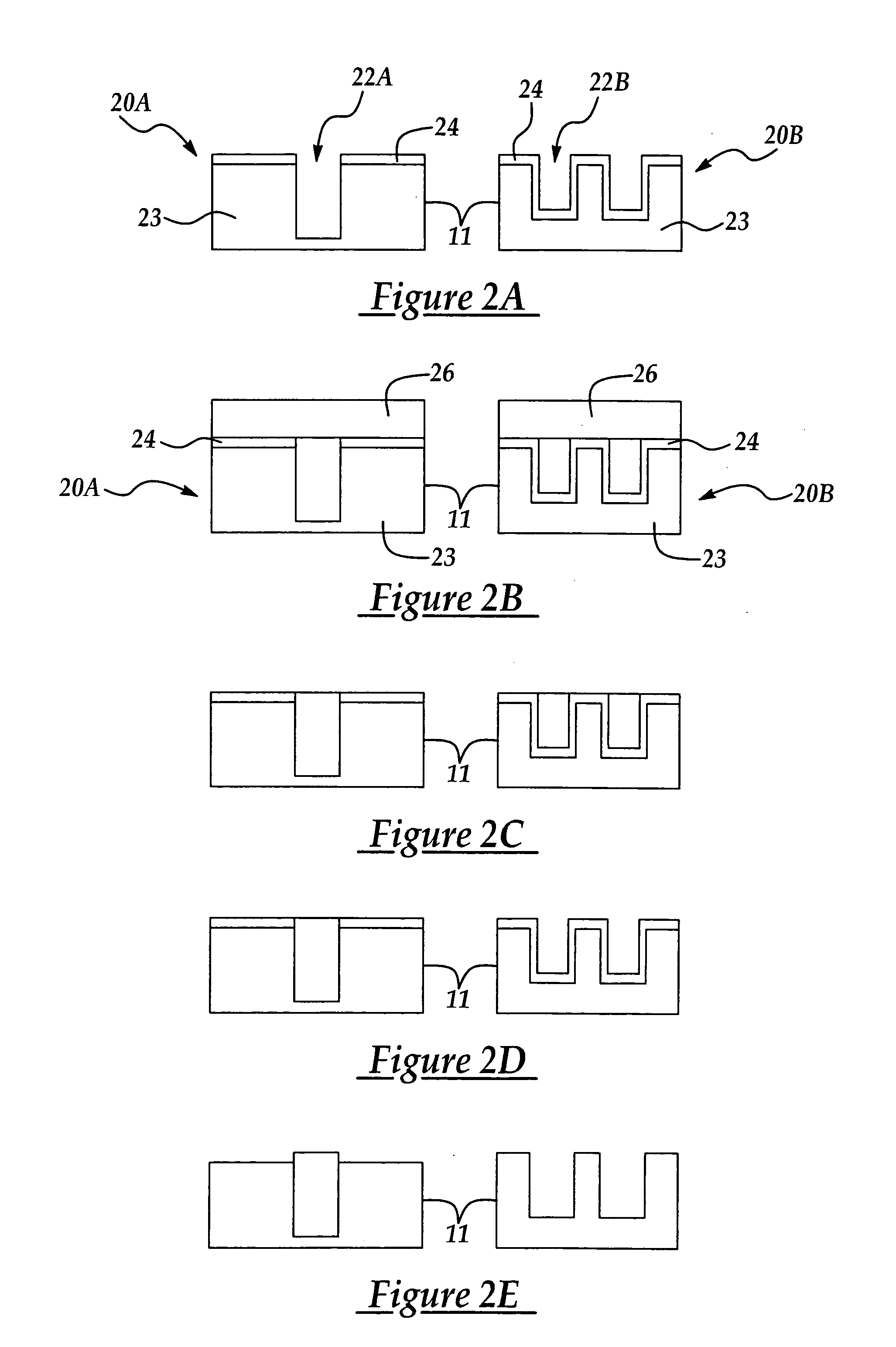
[0023] The method of the present invention is explained with respect to the parallel effect of various processing steps of an active area of a semiconductor process wafer on alignment mark areas, for example global alignment mark areas (fields) disposed at the peripheral portions of the semiconductor process wafer. For example, the method of the present invention is explained with reference to the parallel effects of active area processing on alignment mark areas in connection with the formation of shallow trench isolation (STI) features and subsequent processing steps commonly used for forming CMOS semiconductor features. It will be appreciated that the method of the present invention may be applied to replicate (reproduce) readable alignment marks in any alignment mark field (area) following the deposition of any material layer in a semiconductor wafer processing step where an alignment mark area is advantageously replicated or reproduced without the need for a separate wafer phot...


PUM

PropertyMeasurementUnit
diameteraaaaaaaaaa
diameteraaaaaaaaaa
diameteraaaaaaaaaa

Abstract

A method and apparatus for locally etching a substrate area the method including providing a substrate comprising a process surface; depositing a material layer over the process surface; and, applying a wet etchant to cover a targeted etching portion of the process surface while excluding an adjacent surrounding area to selectively etch the material layer overlying the targeted etching portion.

Description

FIELD OF THE INVENTION [0001] This invention generally relates to semiconductor processing methods including photolithographic patterning and more particularly to a method for replicating alignment marks according to a micro-etching process for improving overlay accuracy in semiconductor wafer photolithography. BACKGROUND OF THE INVENTION [0002] In the integrated circuit industry today, hundreds of thousands of semiconductor devices are built on a single chip. Every device on the chip must be electrically isolated to ensure that it operates independently without interfering with another. With the high integration of the semiconductor devices, the accuracy of formation of feature patterns overlying a previously defined semiconductor device level is increasingly difficult as critical dimensions shrink. Overlay accuracy, also referred to as registration is critical to proper functioning of a semiconductor device. To successfully pattern an overlying feature level on the wafer, the wafe...

Claims


Application Information

Patent Timeline
Patent Type & Authority Applications(United States)
IPC IPC(8): H01L21/00H01L21/302H01L21/311H01L21/336H01L21/461H01L23/544
CPCH01L21/31111H01L21/67282H01L23/544H01L2223/5446H01L2223/54453H01L2223/54426H01L2223/5442H01L2924/0002H01L2924/00
Inventor LIN, YU-LIANGLO, HENRYCHANG, CHUNG-LONGHUANG, GORGELU, TONYYEH, GNESHLIANG, CANDYLIN, CHUN-HSIENZHOU, MEI SHENGWU, SUNNYLIU, AI-SENHUANG, CHENG-LINCHEN, LI-JUIWANG, SHIH CHE
Owner TAIWAN SEMICON MFG CO LTD
Why Eureka
Try Eureka