Semiconductor test apparatus for simultaneously testing plurality of semiconductor devices

a test apparatus and semiconductor technology, applied in the direction of individual semiconductor device testing, testing circuits, instruments, etc., can solve the problems of increasing production costs, and achieve the effect of simplifying the construction of conventional automated test equipmen

Inactive Publication Date: 2005-12-22
UNITEST
View PDF53 Cites 19 Cited by
  • Summary
  • Abstract
  • Description
  • Claims
  • Application Information

AI Technical Summary

Benefits of technology

[0014] Accordingly, the present invention has been made keeping in mind the above problems occurring in the prior art, and an object of the present invention is to provide a semiconductor test apparatus for simultaneously testing a plurality of semiconductor devices, which mainly performs cell and core tests and a direct current test that are most important and require the longest test time among memory tests, except for memory tests having complicated functions in a conventional memory module or memory component, for example, an alternating current margin test or timing generator, and which, in particular, simplifies the construction of conventional automated test equipment in a function test using test patterns and utilizes a programmable device, in which functions, such as pattern generation or comparison or signal application, are implemented on one chip, thus miniaturizing a semiconductor test apparatus and reducing the production cost thereof.

Problems solved by technology

Such a conventional memory tester is disadvantageous in that it performs a DC test for examining whether DC parameters are suitable for the digital operation of the circuit and an Alternating Current (AC) margin test related to the transfer delay time, set-up time and hold time of signals, has various functions, such as a timing generator, for these tests, and is produced using bulky and expensive dedicated equipment, such as a mainframe, thus increasing the production cost.

Method used


Image

  • Semiconductor test apparatus for simultaneously testing plurality of semiconductor devices
  • Semiconductor test apparatus for simultaneously testing plurality of semiconductor devices
  • Semiconductor test apparatus for simultaneously testing plurality of semiconductor devices

Examples


Embodiment Construction

[0030] Hereinafter, embodiments of a semiconductor test apparatus for simultaneously testing a plurality of semiconductor devices according to the present invention will be described in detail with reference to the attached drawings.

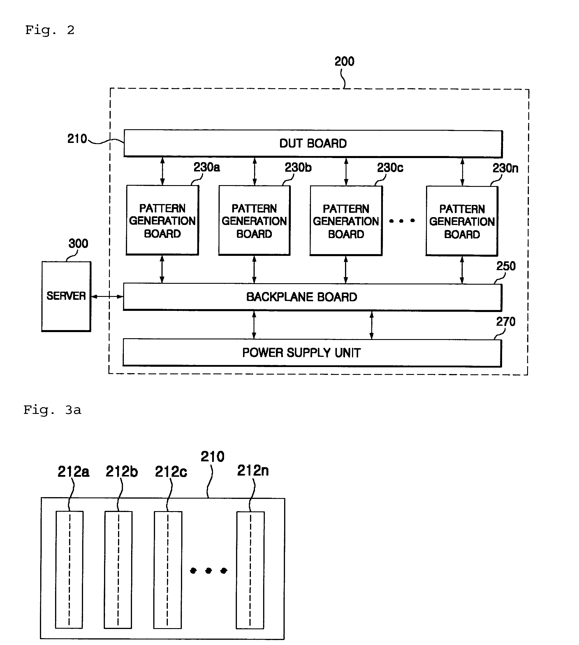
[0031]FIG. 2 is a view showing a simplified construction of a semiconductor test apparatus according to the present invention. As shown in FIG. 2, a semiconductor test apparatus 200 according to the present invention includes a Device Under Test (DUT) board 210, a plurality of pattern generation boards 230a to 230n, a backplane board 250 and a power supply unit 270. Further, the semiconductor test apparatus 200 of the present invention may be connected to an external server 300.

[0032] The external server 300 provides a predetermined user interface and thus provides an environment allowing a user to create a test program that meets the characteristics of semiconductor devices (modules or components) to be tested. Further, the server 300 can provide a us...


PUM


Abstract

Disclosed herein is a semiconductor test apparatus for simultaneously testing a plurality of semiconductor devices. The semiconductor test apparatus includes a plurality of pattern generation boards, a DUT board, a backplane board, and a power supply unit. The pattern generation boards receive a test program, generate a test pattern signal and an expected signal, transmit the test pattern signal to the semiconductor devices, receive a test pattern result signal, compare the test pattern result signal with the expected signal, generate a Direct Current (DC) test signal and a DC test expected signal, transmit the DC test signal to the semiconductor devices, receive a DC test result signal and compare the DC test result signal with the DC test expected signal. The DUT board includes a plurality of sockets for connection to the semiconductor devices and a plurality of connectors for connection to the pattern generation boards. The DUT board receives the test pattern signal or the DC test signal, transmits the received signal to the semiconductor devices, receives the test pattern result signal or DC test result signal and transmits the received signal to the pattern generation boards. The backplane board includes a plurality of connectors for connection to the plurality of pattern generation boards and a communication interface unit, and mechanically supports the pattern generation boards. The power supply unit mechanically supports the backplane board and supplies power to the backplane board.

Description

RELATED APPLICATIONS [0001] The present disclosure relates to subject matter contained in priority Korean Application No. 10-2004-0045421 and 10-2004-0045422, filed on 18 Jun. 2004, which are herein expressly incorporated by reference in its entirety. BACKGROUND OF THE INVENTION [0002] 1. Field of the Invention [0003] The present invention relates, in general, to a semiconductor test apparatus for simultaneously testing a plurality of semiconductor devices and, more particularly, to a semiconductor test apparatus for simultaneously testing a plurality of semiconductor devices, which mainly performs cell and core tests and a direct current test that are most important and require the longest test time among memory tests, except for memory tests having complicated functions in a conventional memory module or memory component, for example, an alternating current margin test or timing generator, and which, in particular, simplifies the construction of conventional automated test equipme...

Claims


Application Information

Patent Timeline
Patent Type & Authority Applications(United States)
IPC IPC(8): G01R31/28G01R31/3193G06F11/00G06F11/263
CPCG06F11/263G01R31/31932
Inventor KANG, JONG KOOKIM, SUN WHAN
Owner UNITEST
Why Eureka
Try Eureka