

Dry-etching method and apparatus
a dry-etching apparatus and dry-etching technology, applied in the direction of electrical equipment, decorative arts, electric discharge tubes, etc., can solve the problems of high resist etching rate of resist materials, large roughness of line edges caused by resist damage, so as to achieve low resistance damage and low etching durability. , the effect of effective suppression of resist damag
- Summary
- Abstract
- Description
- Claims
- Application Information
AI Technical Summary
Benefits of technology
Problems solved by technology
Method used
Image

Examples
embodiment 1
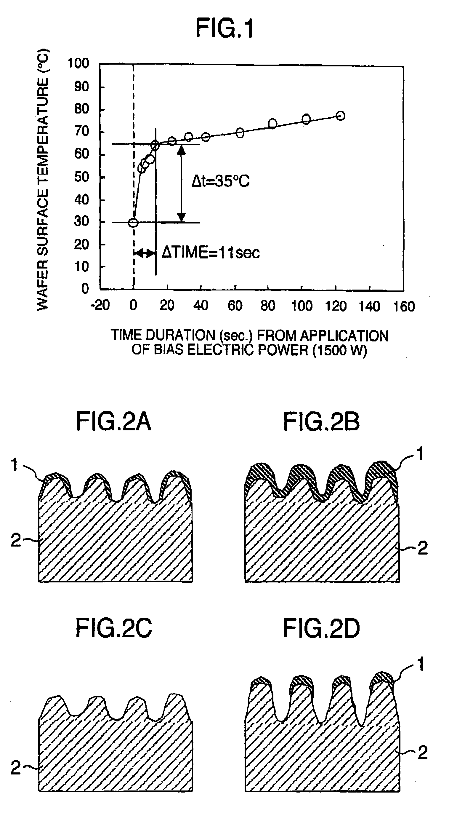
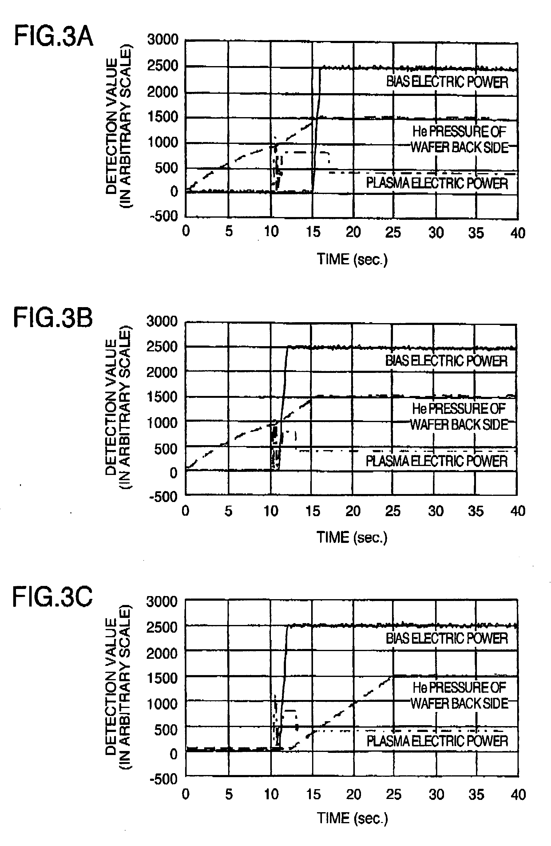
[0044] In Embodiment 1 of the present invention, an explanation is made of a method capable of reducing striation which is caused by resist damage by changing both timing defined after plasma is ignited until bias electric power is turned ON, and timing for conducting helium of a wafer back-side. FIG. 1 graphically represents a relationship between a time duration defined after bias electric power has applied to a wafer, which has been measured when a contact is processed, and a surface temperature of the wafer. It should be noted that a size of the wafer is 8 inches, and a setting value of the bias electric power is 1500 W. As represented in this drawing, under such an etching condition that bias electric power is relatively high, a surface temperature of the wafer is mainly determined by bias electric power. Under this etching condition, the following fact can be seen. That is, the surface temperature of the wafer is higher than a surface temperature thereof before the bias electr...
embodiment 2
[0051] A description is made of Embodiment 2 according to the present invention, in which while an amount of radicals contained in plasma is monitored, a deposition suppressing step for an initial stage of an etching process operation is controlled. FIG. 8 represents such a result that plasma is ignited under condition that a wall of a vacuum chamber is cool, and then, an emission intensity ratio C2 / O ratio is monitored. In this monitoring result, an attention was paid to “C2” as a radical seed of a carbon-series deposition, and also, paid to “O” as a radical seed for removing a deposited seed. The following fact can be understood. That is, up to approximately 200 seconds after a discharging operation was commenced, since the wall of the vacuum chamber is cool, the radicals contained in the plasma are absorbed to the wall, so that a smaller emission intensity ratio value than the original emission intensity ratio value is represented. After 200 seconds, the absorption of the radical...
embodiment 3
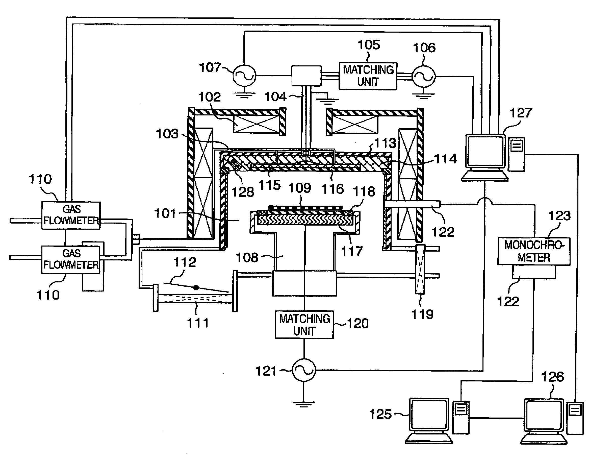
[0055] In Embodiment 3 of the present invention, a description is made of such an embodiment that a temperature of a wafer is increased before a process operation is carried out, while a process condition is not changed. FIG. 10 is a diagram for schematically showing an etching system. In this etching system, after a wafer 206 has been derived from a cassette, this wafer 206 is transported via a step for executing an alignment control to a load lock chamber 201 where air is sucked in a vacuum sucking manner. Thereafter, the wafer 206 is conducted via a buffer chamber 202 into an etching chamber 204. After a predetermined process operation is carried out in the etching chamber 204, the wafer 206 is transported from an unload lock chamber 205 outside the apparatus. Embodiment 3 has described such an example that the alignment control is carried out in an atmospheric condition. Alternatively, this alignment control may be carried out in a vacuum condition. Embodiment 3 is featured by t...
PUM
| Property | Measurement | Unit |
|---|---|---|
| pressure | aaaaa | aaaaa |
| time duration | aaaaa | aaaaa |
| size | aaaaa | aaaaa |
Abstract
Description
Claims
Application Information