

Structures and methods for manufacturing p-type mosfet withgraded embedded silicon-germanium source-drain and/or extension
a technology of source-drain and mosfet, which is applied in the direction of semiconductor devices, electrical apparatus, transistors, etc., can solve the problems of difficult production of dislocations, and achieve the effect of improving the mobility of holes
- Summary
- Abstract
- Description
- Claims
- Application Information
AI Technical Summary
Benefits of technology
Problems solved by technology
Method used
Image

Examples
Embodiment Construction
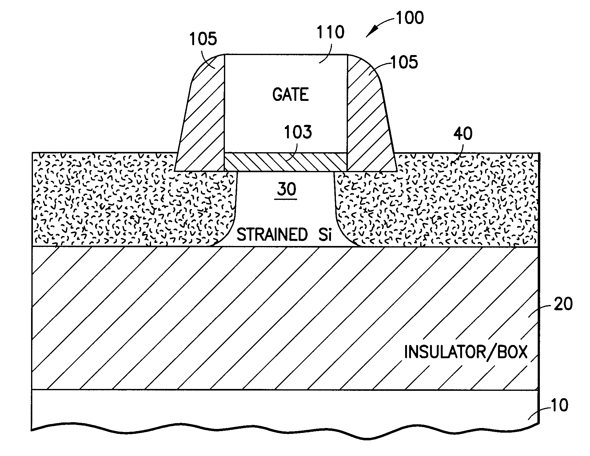
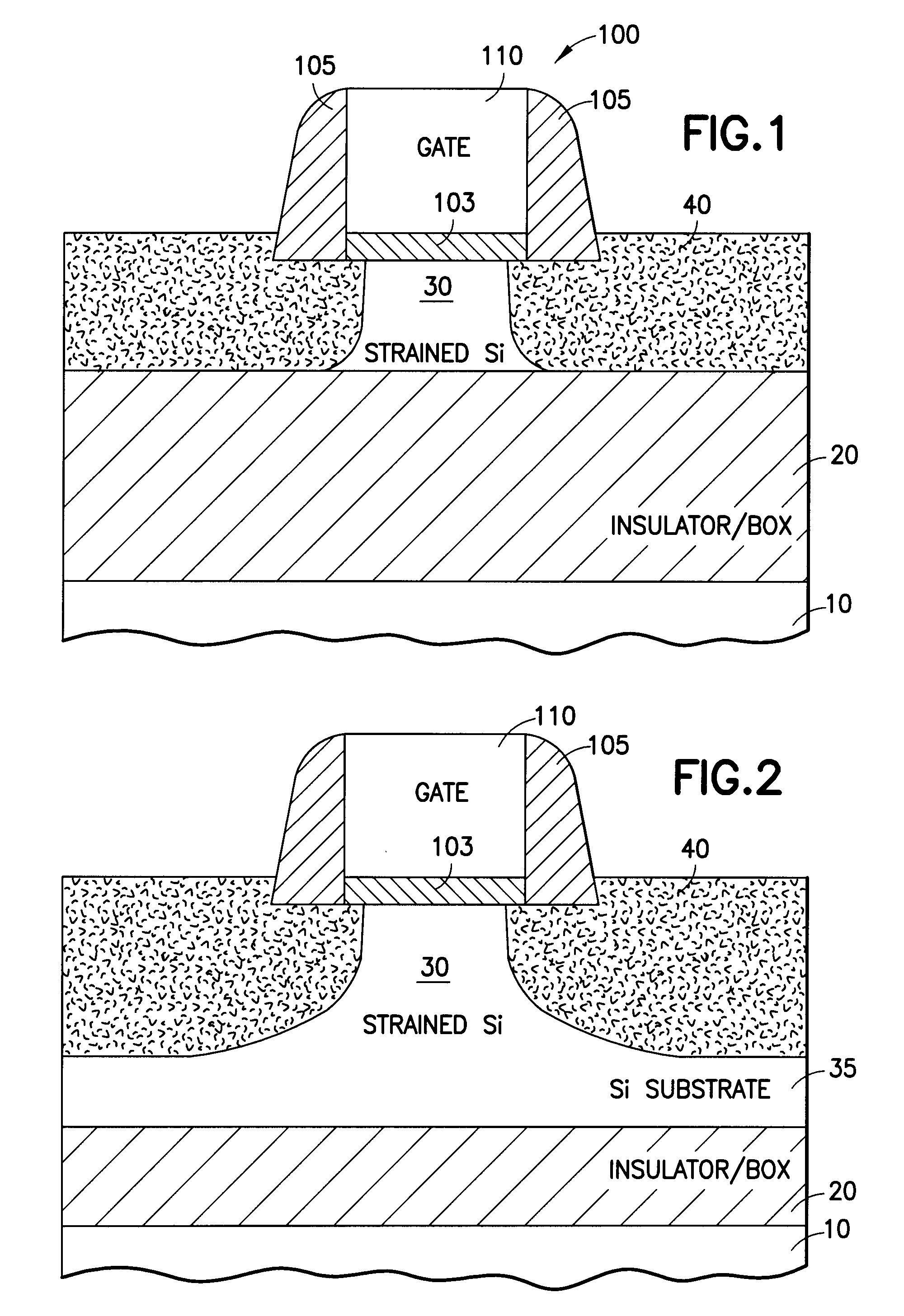
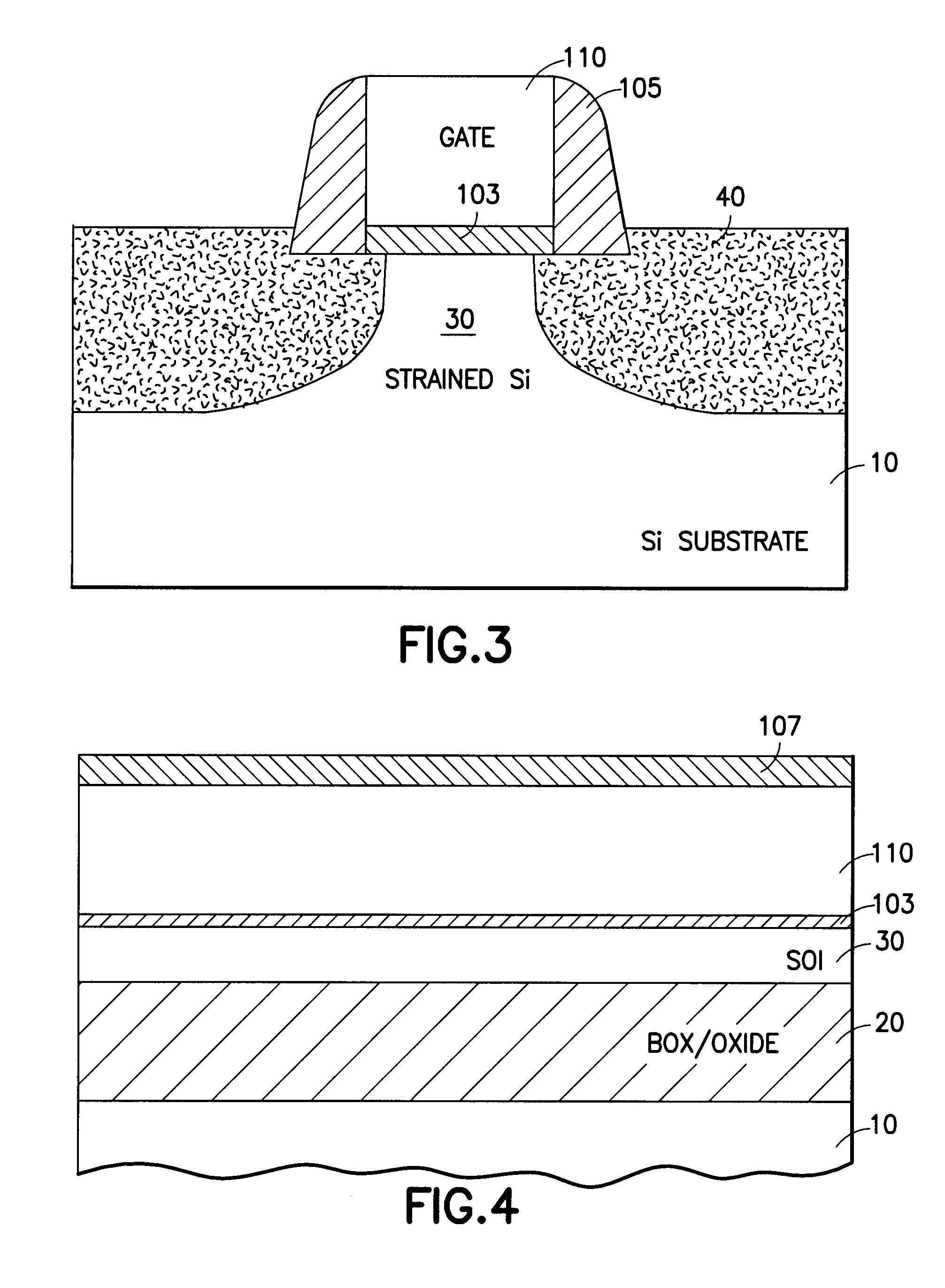
[0023]FIG. 1 shows in cross section a simplified field effect transistor 100 formed in a portion of a silicon wafer 10 having a buried insulator layer 20 and a device layer of silicon or semiconductor (or an SOI layer) 30. Transistor gate 110 and sidewalls 105 are positioned above gate oxide 103 that defines the lateral extent of body 30. Source and drain 40 are formed from portions of the SOI layer 30 that have been doped with germanium in a previous step. The germanium has diffused downward toward the insulator layer 30 and inward to the center of the channel under the gate. This has imposed compressive stress in the horizontal direction (parallel to the SOI surface) in the SOI and tensile stress in vertical direction (normal to the SOI surface) in the center of the device. These components complete a field effect transistor that illustratively has an n-type body that forms a channel for p-type field effect transistor (PMOSFET).
[0024] A PFET is shown for illustration. Typically, ...
PUM
| Property | Measurement | Unit |
|---|---|---|
| thickness | aaaaa | aaaaa |
| thick | aaaaa | aaaaa |
| thick | aaaaa | aaaaa |
Abstract
Description
Claims
Application Information