

Planar motor initialization method, planar motro, lithographic apparatus and device manufacturing method
- Summary
- Abstract
- Description
- Claims
- Application Information
AI Technical Summary
Benefits of technology
Problems solved by technology
Method used
Image

Examples
Embodiment Construction
Lithographic Apparatus
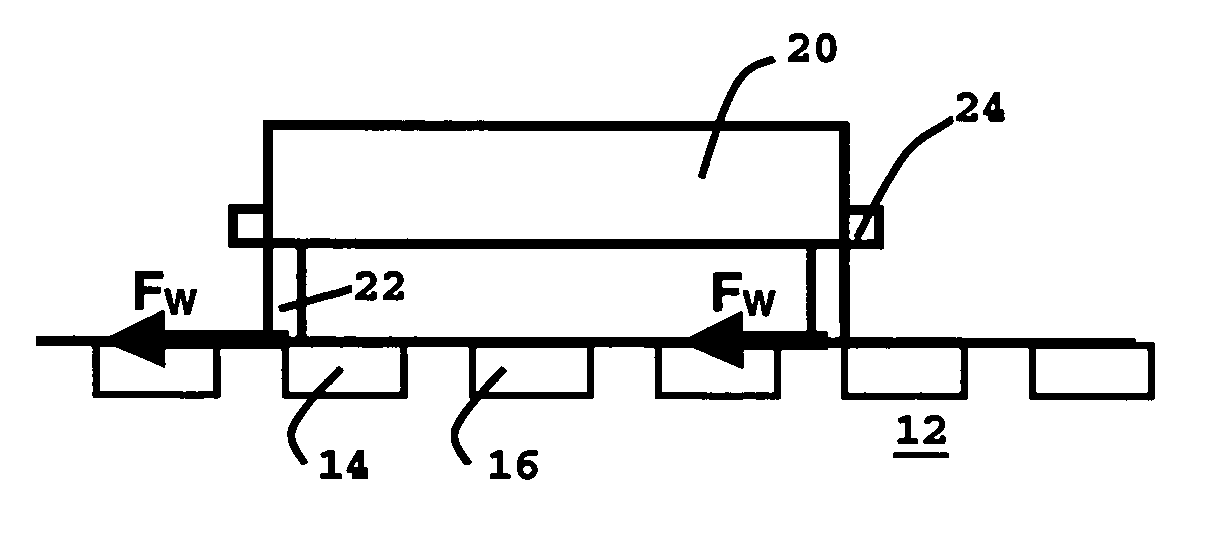
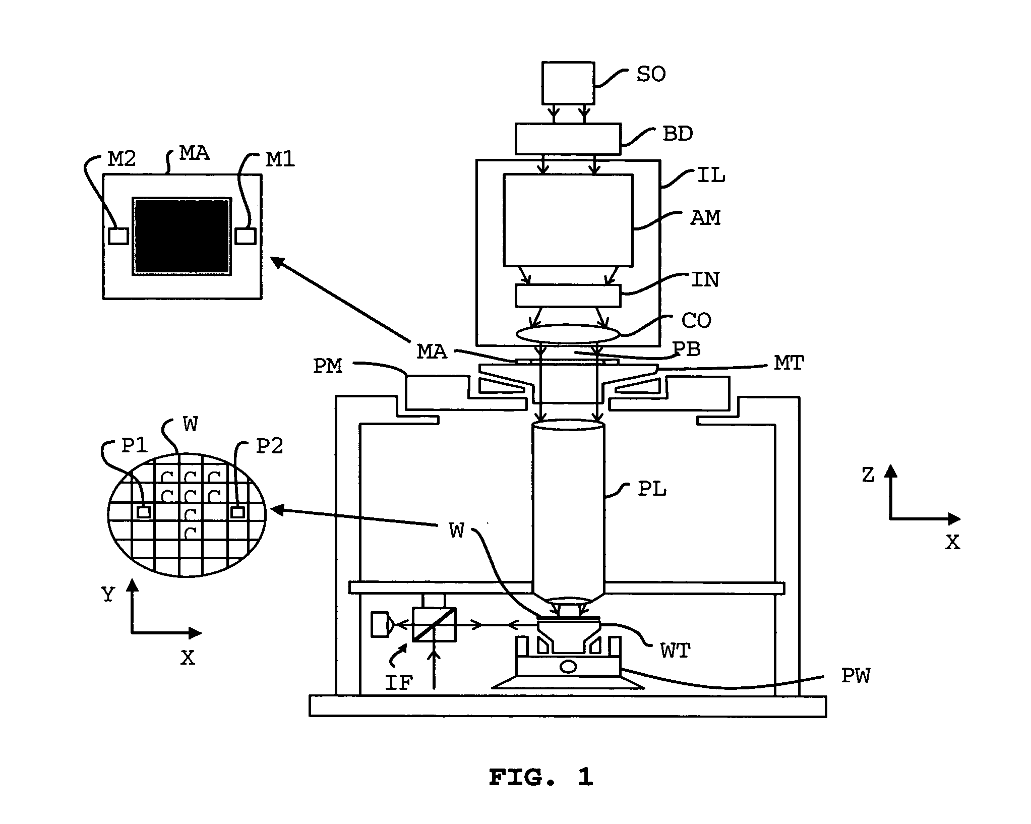
[0045]FIG. 1 schematically depicts a lithographic apparatus 1 according to an embodiment of the invention. The apparatus comprises:
[0046] The apparatus 1 comprises: [0047] an illumination system (illuminator) IL: for providing a projection beam PB of radiation (e.g. UV or EUV radiation). [0048] a first support structure (e.g. a mask table / holder) MT: for supporting patterning device (e.g. a mask) MA and coupled to first positioning mechanism PM for accurately positioning the patterning device with respect to item PL; [0049] a substrate table (e.g. a wafer table / holder) WT: for holding a substrate (e.g. a resist-coated wafer) W and coupled to second positioning mechanism PW for accurately positioning the substrate with respect to item PL; and [0050] a projection system (e.g. a reflective projection lens) PL: for imaging a pattern imparted to the projection beam PB by patterning device MA onto a target portion C (e.g. comprising one or more dies) of the substr...
PUM
 Abstract
Description
Claims
Application Information