Method of producing multi-wavelength semiconductor laser device

a laser device and multi-wavelength technology, applied in the direction of semiconductor laser structure details, semiconductor laser arrangements, semiconductor lasers, etc., can solve the problems of not being able to apply to a three-wavelength (further including light of a short wavelength) semiconductor laser device, unable to form on the same substrate, and difficult to grow algainp and gan epitaxial layers on the same substra

Inactive Publication Date: 2005-12-29
SAMSUNG ELECTRO MECHANICS CO LTD
View PDF20 Cites 127 Cited by
  • Summary
  • Abstract
  • Description
  • Claims
  • Application Information

AI Technical Summary

Benefits of technology

[0028] In order to integrate the semiconductor laser structures composed of the respective epitaxial layers, which are grown under different conditions, into one chip, the multi-wavelength semiconductor laser device of the present invention is produced by forming the respective nitride epitaxial layers for the first and second semiconductor laser structures oscillating light of short wavelengths, separating the nitride epitaxial layers from each other, attaching the separated epitaxial layers to the first conductivity-type substrate, and forming the third semiconductor laser structure on the first conductivity

Problems solved by technology

As explained earlier in FIGS. 1a to 1g, the conventional method is limited to the two-wavelength (650 nm and 780 nm) semiconductor laser device, and thus cannot be applied to a three-wavelength (further including light of a short wavelength) semiconductor laser device.
In this connection, there is a problem that since GaN-based epitaxial layers are particularly required to produce a semiconductor laser device oscillating light at wavelengths of 460 nm and 530 nm, they cannot be formed on the same substrate, together with a semiconductor laser structure oscillating light at a wavelength of 635 nm.

Method used


Image

  • Method of producing multi-wavelength semiconductor laser device
  • Method of producing multi-wavelength semiconductor laser device
  • Method of producing multi-wavelength semiconductor laser device

Examples


Embodiment Construction

[0032] Detailed description will be made of the preferred embodiment of the present invention with reference to the accompanying drawings.

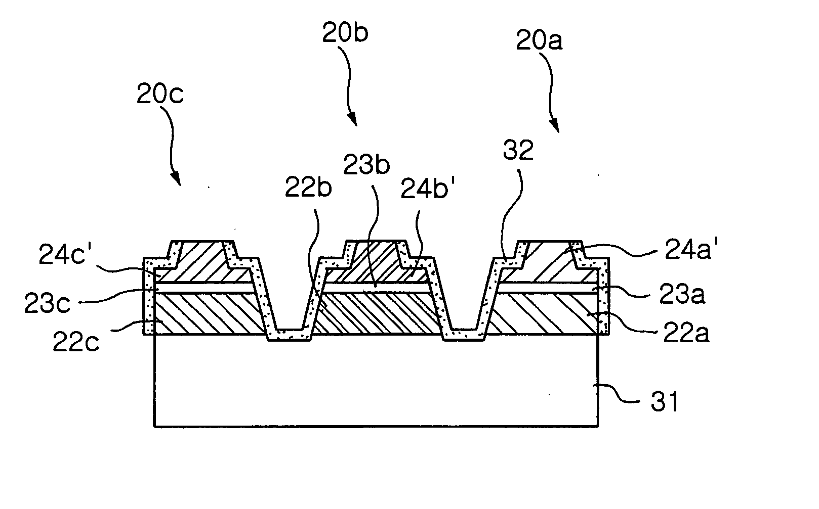
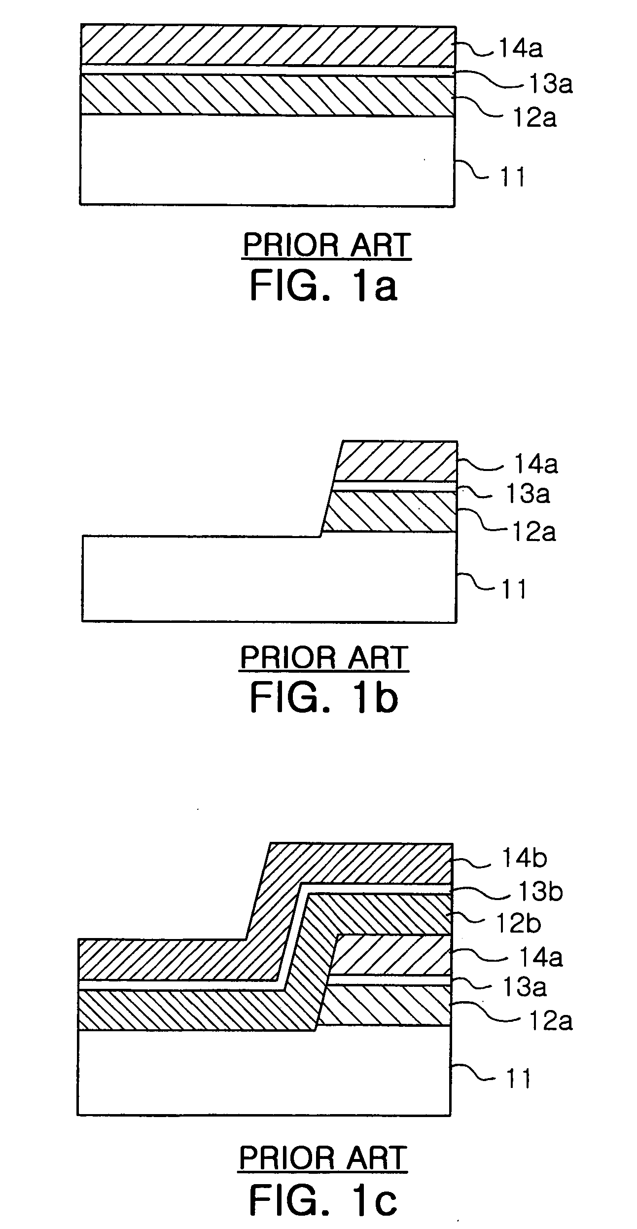
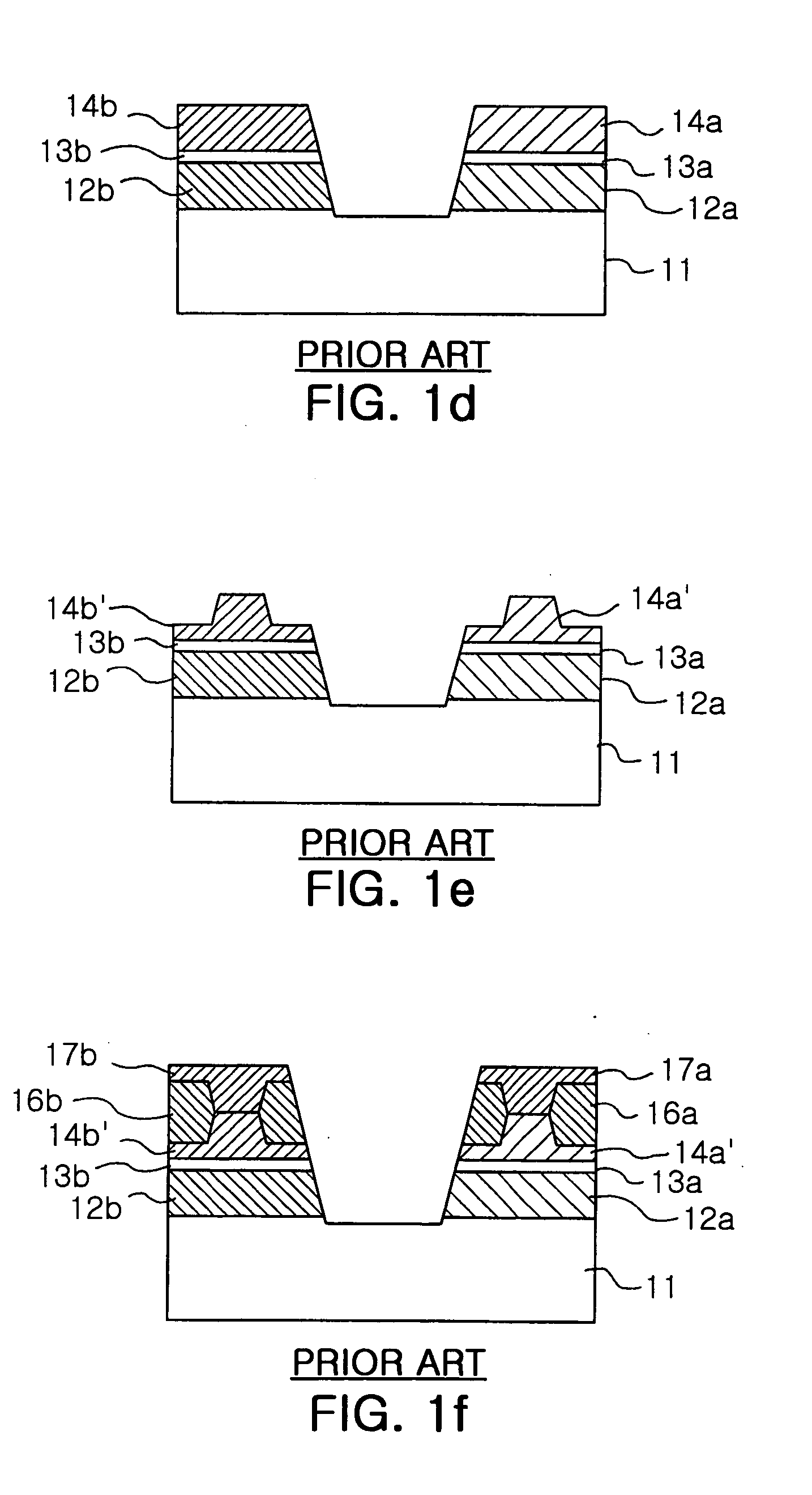
[0033]FIGS. 2a to 2l are cross-sectional views illustrating the overall procedure of a method for producing a three-wavelength semiconductor laser device according to a preferred embodiment of the present invention.

[0034] As shown in FIG. 2a, a first nitride epitaxial layer 25a for a semiconductor laser structure oscillating light of a short wavelength (e.g., 460 nm) is formed on a sapphire substrate 21. The first nitride epitaxial layer 25a can be formed by sequentially growing a first conductivity-type first clad layer 22a, a first active layer 23a and a second conductivity-type first clad layer 24a. The first conductivity-type first clad layer 22a may be composed of an n-type Al0.2Ga0.8N layer and an n-type GaN layer, and the second conductivity-type first clad layer 24a may be composed of a p-type Al0.2Ga0.8N layer and a p-type GaN layer. Th...


PUM


Abstract

Disclosed herein is a method for producing a multi-wavelength semiconductor laser device. The method comprises the steps of: forming first and second nitride epitaxial layers in parallel on a substrate for growth of a nitride single crystal; separating the first and second nitride epitaxial layers from the substrate; attaching the separated first and second nitride epitaxial layers to a first conductivity-type substrate; selectively removing the first and second nitride semiconductor epitaxial layers to expose a portion of the first conductivity-type substrate and to form first and second semiconductor laser structures, respectively; and forming a third semiconductor laser structure on the exposed portion of the first conductivity-type substrate.

Description

BACKGROUND OF THE INVENTION [0001] 1. Field of the Invention [0002] The present invention relates to a multi-wavelength semiconductor laser device, and more particularly to a multi-wavelength semiconductor laser device capable of simultaneously or selectively oscillating laser light of three different wavelengths (e.g., 460 nm, 530 nm and 635 nm), and a method for producing the multi-wavelength semiconductor laser device. [0003] 2. Description of the Related Art [0004] In general, a semiconductor laser device is one that produces light amplified by stimulated emission of radiation. The light produced by the semiconductor laser device has a narrow frequency width (one of short-wavelength characteristics), superior directivity and high output. Due to these advantages, the semiconductor laser device is used as a light source for an optical pick-up apparatus of an optical disc system, such as a CD (compact disc) or DVD (digital video disc) player, as well as, is widely applied to a wide...

Claims


Application Information

Patent Timeline
IPC IPC(8): H01S5/30H01S5/00H01S5/02H01S5/22H01S5/323H01S5/40
CPCH01S5/0213H01S5/0215H01S5/40H01S5/22H01S5/32341H01S5/0217H01S5/4087H01S5/30
Inventor LEE, SANG DON
Owner SAMSUNG ELECTRO MECHANICS CO LTD
Why Eureka
Try Eureka