Thin film transistor (TFT) and flat panel display including the TFT and their methods of manufacture

a technology of thin film transistors and flat panel displays, which is applied in the direction of basic electric elements, electrical apparatus, and semiconductor devices, can solve the problems of signal delay in flat panel displays including tfts, and reduce the picture quality of flat panel displays, so as to reduce interconnection resistance, prevent contamination, and reduce contact resistance

Inactive Publication Date: 2006-01-05
SAMSUNG SDI CO LTD
View PDF15 Cites 27 Cited by
  • Summary
  • Abstract
  • Description
  • Claims
  • Application Information

AI Technical Summary

Benefits of technology

[0012] The present invention provides a thin film transistor (TFT) which reduces interconnection resistance of source / drain electrodes, prevents contamination from an active layer, reduces contact resistance between a pixel electrode and the source / drain electrodes, smoothly supplies hydrogen to the active layer and has high mobility, on-current characteristics, and threshold voltage characteristics, and a flat panel display device having the TFT.

Problems solved by technology

Since molybdenum has a high specific resistance, the resistance of the source / drain electrodes and the signal interconnection is increased, resulting in a signal delay in a flat panel display including the TFT.
This signal delay causes the lowering of the picture quality of the flat panel display.

Method used


Image

  • Thin film transistor (TFT) and flat panel display including the TFT and their methods of manufacture
  • Thin film transistor (TFT) and flat panel display including the TFT and their methods of manufacture
  • Thin film transistor (TFT) and flat panel display including the TFT and their methods of manufacture

Examples


Embodiment Construction

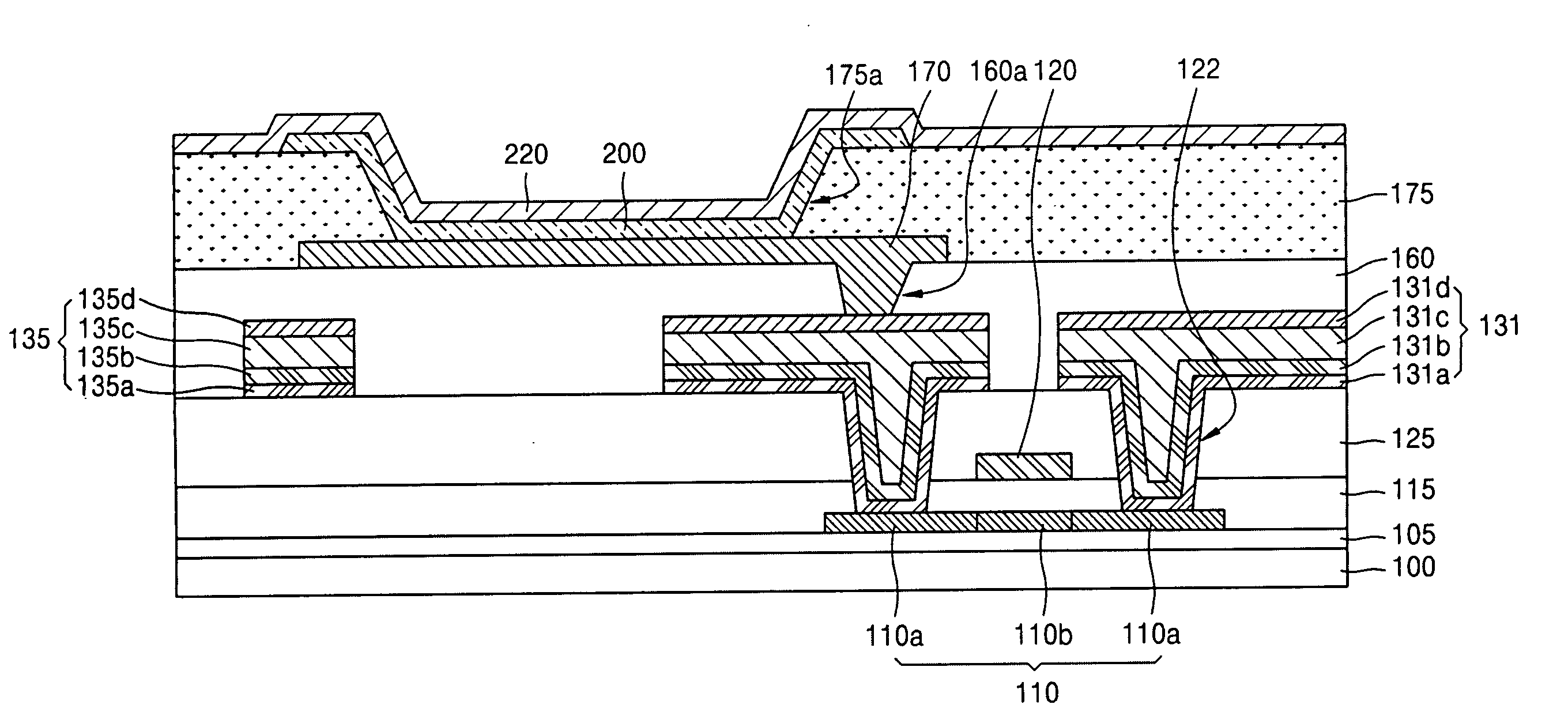
[0043]FIG. 1 is a cross-sectional view of a TFT of a flat panel display. Referring to FIG. 1, an active layer 20 comprised of a semiconductor is formed on a substrate 10. A gate insulating layer 30 is formed on the active layer 20 to cover the active layer 20. A gate electrode 40 is formed on the gate insulating layer 30. The gate electrode 40 is covered with an InterLevel Dielectric (ILD) layer 50, and contact holes 50a through which source / drain regions of the active layer 20 are exposed are formed in the gate insulating layer 30 and the ILD layer 50. Source / drain electrodes 55 are formed on the ILD layer 50. The source / drain electrodes 55 are connected to the source / drain regions of the active layer 20 through the contact holes 50a. When forming the source / drain electrodes 55, a variety of signal interconnections (not shown) of the flat panel display can be formed together.

[0044] The source / drain electrodes 55 and the signal interconnections can be formed of molybdenum or molybd...


PUM


Abstract

A Thin Film Transistor (TFT) reduces interconnection resistance of source/drain electrodes, prevents contamination from an active layer, reduces contact resistance between a pixel electrode and the source/drain electrodes, smoothly supplies hydrogen to the active layer and has high mobility, on-current characteristics, and threshold voltage characteristics The TFT includes an active layer having a channel region and source/drain regions, a gate electrode supplying a signal to the channel region, source/drain electrodes respectively connected to the source/drain regions and including at least one of Ti, a Ti alloy, Ta, and a Ta alloy; and an insulating layer interposed between the source/drain electrodes and the active layer and including silicon nitride.

Description

CROSS-REFERENCE TO RELATED APPLICATIONS [0001] Furthermore, the present application is related to a co-pending U.S. application Ser. No. (to be determined), entitled THIN FILM TRANSISTOR (TFT) AND FLAT PANEL DISPLAY INCLUDING TFT, based upon Korean Patent Application Serial No. 10-2004-0050422 filed in the Korean Intellectual Property Office on 30 Jun. 2004, and filed in the U.S. Patent & Trademark Office concurrently with the present application.CLAIM OF PRIORITY [0002] his application makes reference to, incorporates the same herein, and claims all benefits accruing under 35 U.S.C. § 119 from an application entitled TFT, MANUFACTURING METHOD OF THE TFT, FLAT PANEL DISPLAY DEVICE WITH THE TFT, AND MANUFACTURING METHOD OF FLAT PANEL DISPLAY DEVICE filed with the Korean Industrial Property Office on Jun. 30, 2004 and there duly assigned Serial No. 10-2004-0050421. BACKGROUND OF THE INVENTION [0003] 1. Field of the Invention [0004] The present invention relates to a Thin Film Transist...

Claims


Application Information

Patent Timeline
Patent Type & Authority Applications(United States)
IPC IPC(8): H01L21/00H01L27/01
CPCH01L27/12H01L27/3248H01L27/124H01L29/456H01L27/3279H10K59/123H10K59/1315H01L27/1214H01L29/458
Inventor KIM, TAE-SEONG
Owner SAMSUNG SDI CO LTD
Why Eureka
Try Eureka