

Semiconductor device and a CMOS integrated circuit device
a high-speed semiconductor and integrated circuit technology, applied in the field of semiconductor devices including cmos circuits, can solve the problems of reducing the carrier mobility of the p-channel mos transistor, and achieve the effect of increasing the carrier mobility of the channel region and hence the operational speed of the mos transistor
- Summary
- Abstract
- Description
- Claims
- Application Information
AI Technical Summary
Benefits of technology
Problems solved by technology
Method used
Image

Examples
first embodiment
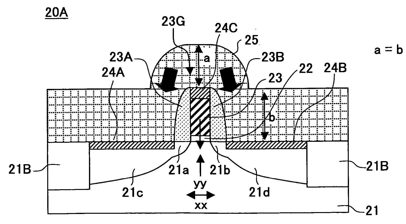
[0082]FIG. 6A shows the construction of an n-channel MOS transistor 20 having a gate length of 37 nm according to a first embodiment of the present invention, while FIG. 6B shows the construction of an n-channel MOS transistor 20A having the identical construction as the MOS transistor 10 of FIG. 1 for the purpose of comparison and for the purpose of explanation of the MOS transistor 20 of FIG. 6A, wherein it should be noted that FIG. 6B shows the transistor 20A by using the same reference numerals used with FIG. 6A.
[0083] Referring to FIG. 6A, there is defined a device region 20A for the n-channel MOS transistor 20 on a silicon substrate 21 by a device isolation region 21B of STI type, and a gate electrode 23 is formed on the device region 20A via an SiON gate insulation film 22.
[0084] Further, there are formed n-type LDD regions 21a and 21b in the silicon substrate 21 at both lateral sides of the gate electrode 23, and source and drain diffusion regions 21c and 21d of n+-type ar...
second embodiment
[0109] Meanwhile, in a semiconductor integrated circuit in which the n-channel MOS transistors are arranged with large number in such a manner that the diffusion regions 21c and 21d are shared by adjacent n-channel MOS transistors, it becomes necessary to decrease the interval between adjacent resist patterns R1 as shown in FIG. 11 at the time of patterning the SiN film 25 with the process of FIGS. 10A and 10B when the thickness of the SiN film 25 is large relative to the repetition pitch of the n-channel MOS transistors. In such a case, however, there arises a problem that exposure of such closely neighboring resist patterns R1 is difficult because of the proximity effect.
[0110] In such a case, it becomes possible to pattern the individual resist patterns R1 by restricting the thickness of the SiN film 25 as shown in FIG. 12A. Thereby, it becomes possible to decrease the thickness of the SiN film in the part located between adjacent MOS transistors.
[0111]FIG. 12B shows a structur...
third embodiment
[0117]FIG. 15 shows the construction of a CMOS device 40 according to a third embodiment of the present invention.
[0118] Referring to FIG. 15, the CMOS device 40 is formed on a silicon substrate 41, wherein the silicon substrate 41 is formed with a device region 41A for an n-channel MOS transistor and a device region 41B for a p-channel MOS transistor by a device isolation structure 41I of STI type.
[0119] On the device region 41A, there is formed a gate electrode 43A doped to n+-type in correspondence to a channel region of the n-channel MOS transistor 40A via a gate insulation film 42A of SiON, and the like, and LDD regions 41a and 41b of n-type are formed in the device region 41A at both lateral sides of the gate electrode 43A.
[0120] Further, sidewall insulation films 43a and 43b are formed on both sidewall surfaces of the gate electrode 43A, and diffusion regions 41c and 41d of n+-type are formed in the device region 41A at the outer sides of the sidewall insulation films 43a ...
PUM
 Abstract
Description
Claims
Application Information