Semiconductor devices, DC/DC converter and power supply

a technology of dc/dc converter and power supply, applied in the direction of electric variable regulation, process and machine control, instruments, etc., can solve the problems of inability to fully prevent self-turning on phenomenon, difficult to replace existing products with disclosed packages, etc., and achieve the effect of greatly improving power conversion efficiency

Active Publication Date: 2006-01-12
RENESAS ELECTRONICS CORP
View PDF6 Cites 46 Cited by
  • Summary
  • Abstract
  • Description
  • Claims
  • Application Information

AI Technical Summary

Benefits of technology

[0034] (1) The self-turn-on phenomenon in a system-in-package for power supply applications can be prevented.
[0035] (2) As a r

Problems solved by technology

Further, the pin configuration of the package is different from that of existing products, making it difficult to replace existing products with the disclosed package.
The inventors' analysis revealed that the self-turn-on phenomenon, which is a problem also in the above-described system-in-pa

Method used


Image

  • Semiconductor devices, DC/DC converter and power supply
  • Semiconductor devices, DC/DC converter and power supply
  • Semiconductor devices, DC/DC converter and power supply

Examples


embodiment 1

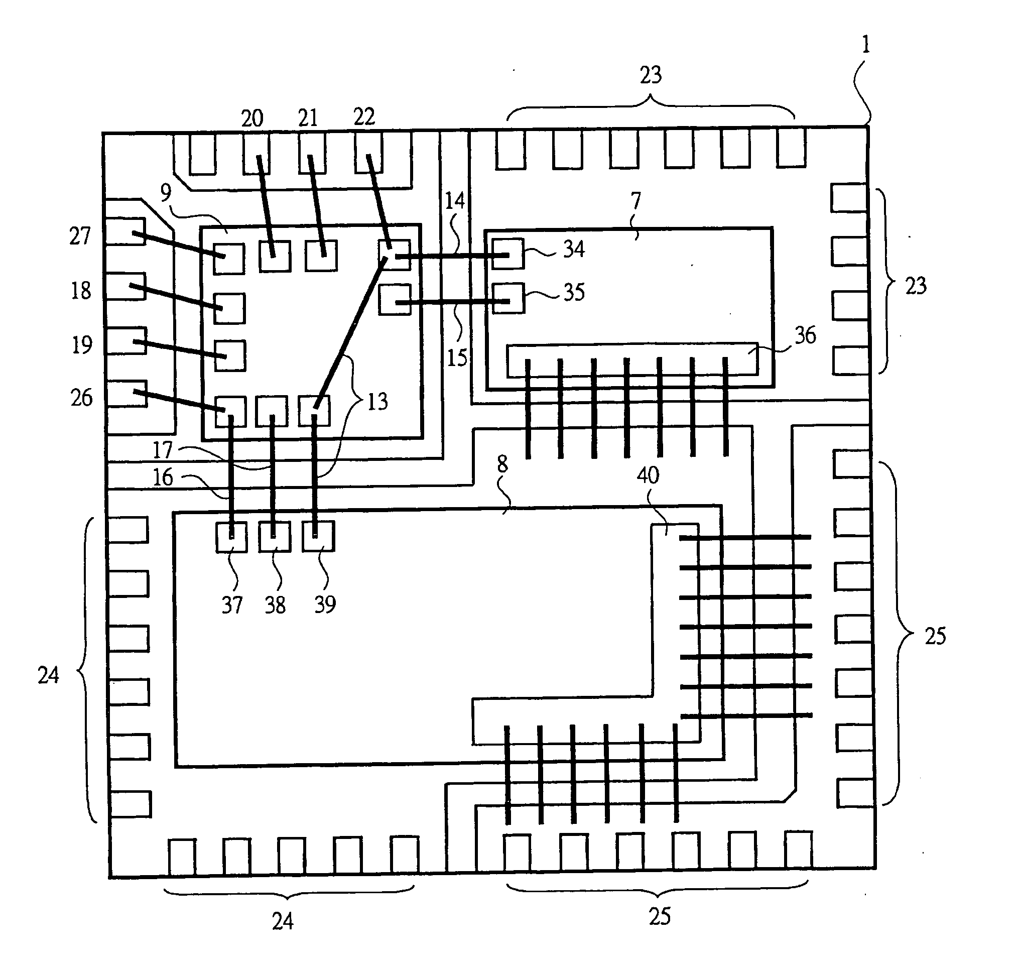
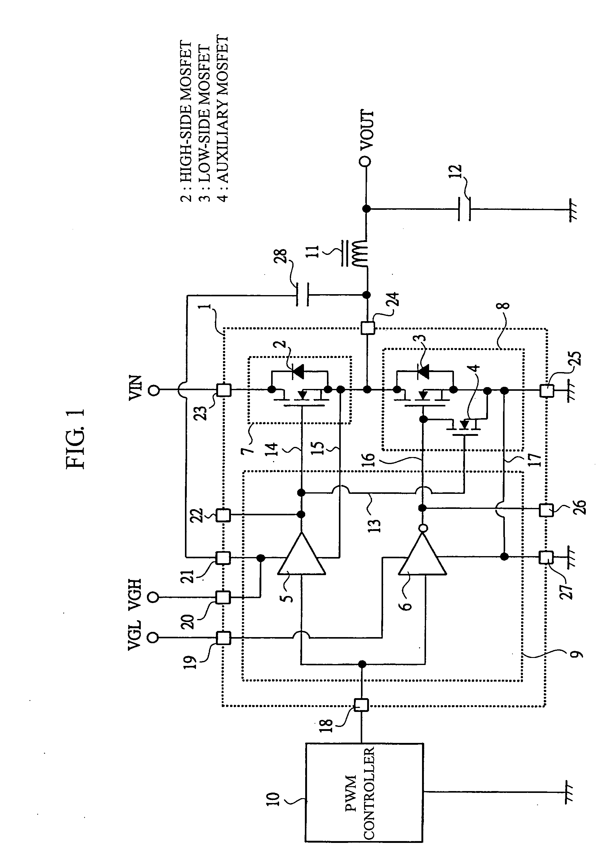
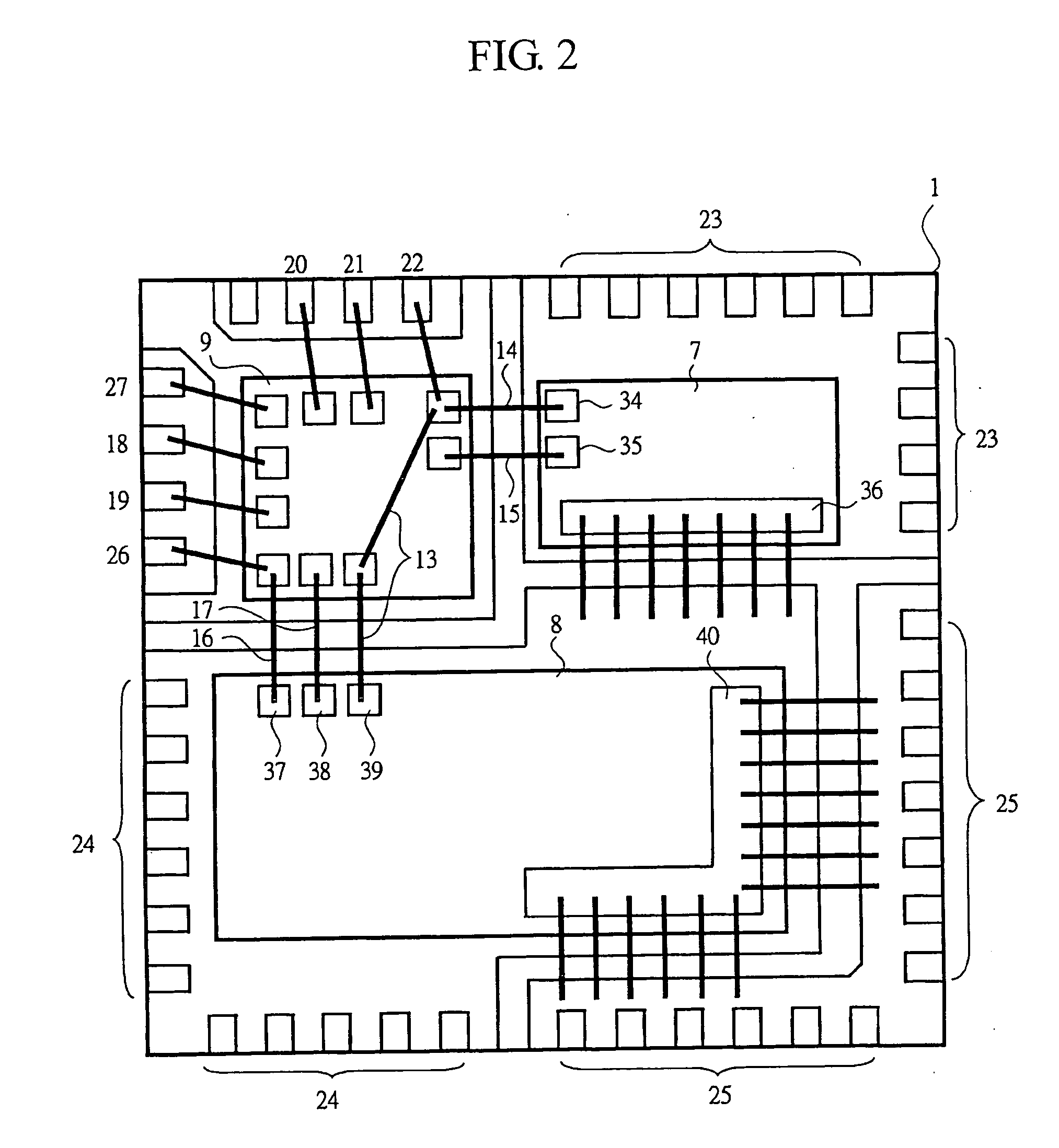
[0050]FIG. 1 shows an example of the circuit configuration of a system-in-package according to a first embodiment of the invention. FIG. 2 shows an example of the package exterior view, chip configuration, and wire bonding configuration of the system-in-package shown in FIG. 1. FIG. 3 shows a timing chart of individual voltages for illustrating the effect of preventing the self-turn-on phenomenon. FIG. 4 shows a simulation result illustrating the effect of the invention. FIG. 5 shows an example of the cross-sectional structure of a device.

[0051]FIG. 1 shows an example of the circuit configuration of the system-in-package of Embodiment 1. It is characterized in that, as compared with the above-described configuration of the conventional circuit shown in FIG. 8, an auxiliary MOSFET 4 for short-circuiting the gate-source junction is fabricated on the same chip as the low-side MOSFET 3. Another feature is that the gate of the auxiliary MOSFET 4 is driven, via a wire 13, by a driver 5 f...

embodiment 2

[0074]FIG. 6 shows an example of the circuit configuration of a system-in-package according to a second embodiment of the invention. FIG. 7 shows an example of the exterior view of the package, chip configuration, and wire bonding configuration of the example shown in FIG. 6.

[0075]FIG. 6 shows an example of the circuit configuration of the system-in-package according to the second embodiment of the invention. The example is based on Embodiment 1 shown in FIG. 1 to which a pre-driver is further added in front of the gate of the low-side MOSFET 3, with the final stage of the pre-driver driving the low-side MOSFET 3 disposed on the same chip. Specifically, in the system-in-package 30 of Embodiment 2, the p-type auxiliary MOSFET 31 for driving the gate of the low-side MOSFET 3 is disposed on the same chip, with the auxiliary MOSFET 31 and another auxiliary MOSFET 4 constituting an inverter. The low-side MOSFET 3 is comprised of a trench vertical power MOSFET, and the auxiliary MOSFETs ...

embodiment 3

[0081]FIGS. 12 and 13 show an example of the circuit configuration of a system-in-package in accordance with a third embodiment of the invention.

[0082] In Embodiment 1, the auxiliary switch is driven by the driver for driving the high-side switch. In Embodiment 3, in order to reduce the driving voltage for the auxiliary switch, the auxiliary switch is driven with:

[0083] (1) a signal obtained by reducing the level of the output of the driver for driving the high-side switch; or

[0084] (2) a driver signal in a stage prior to the final stage of the driver for driving the low-side switch.

[0085]FIG. 11 shows an example of the circuit configuration of the system-in-package according to Embodiment 1 for DC / DC converters, illustrating the driver unit for driving the MOSFETs in detail. The driver 5 for driving the high-side switch is made up of: a p-type MOSFET 53 and an n-type MOSFET 54 that constitute the final portion of the driver output stage; drivers 55, 56, and 57 in an earlier sta...


PUM


Abstract

A semiconductor device in which the self-turn-on phenomenon is prevented that can significantly improve power conversion efficiency. The semiconductor device is a system-in-package for power supply applications in which a high-side switch, a low-side switch, and two drivers are included in a single package. The device includes an auxiliary switch disposed between the gate and source of said low-side switch, and a low-side MOSFET 3 for the low-side switch and an auxiliary MOSFET 4 for the auxiliary switch are disposed on the same chip. In this way, the self-turn-on phenomenon can be prevented, allowing the mounting of a low-side MOSFET 3 with a low threshold voltage and thereby significantly improving power conversion efficiency. The gate of the auxiliary MOSFET 4 is driven by the driver for the high-side MOSFET 2, thereby eliminating the need for a new drive circuit and realizing the same pin configuration as existing products, which facilitates easy replacement.

Description

BACKGROUND OF THE INVENTION [0001] 1. Field of the Invention [0002] The present invention relates to a semiconductor device in a power supply circuit, and more particularly to a technique for improving power conversion efficiency in a semiconductor device used in DC / DC converters that is referred to as a system-in-package, in which a high-side switch, a low-side switch, and a driver are included in a single package. [0003] 2. Background Art [0004] The following is an analysis of the technologies relating to semiconductor devices in power supply circuits. [0005] In response to the growing demand for smaller size and faster load response in power supply circuits, the frequencies of the power MOSFETs (Metal Oxide Semiconductor Field Effect Transistors) used in power supplies are becoming increasingly higher. [0006] In particular, there is a growing tendency to increase current levels and frequencies in the non-isolated DC / DC converters used in the power supply circuits for personal com...

Claims


Application Information

Patent Timeline
IPC IPC(8): H01L29/76H01L21/822H01L27/04H02M3/155
CPCH01L21/823487H01L2924/1306H01L27/088H01L29/7813H02M3/1588Y02B70/1466H01L2924/13091H01L25/16H01L2924/30107H01L2224/49111H01L2224/4813H01L2224/0603H01L2224/48137H01L2224/49175H01L24/49H01L2924/00H01L2224/05554H01L2924/00014H01L24/48Y02B70/10H01L2224/45099H01L2224/05599
Inventor SHIRAISHI, MASAKIIWASAKI, TAKAYUKIMATSUURA, NOBUYOSHI
Owner RENESAS ELECTRONICS CORP
Why Eureka
Try Eureka