Solid-state imaging device, camera and method of producing the solid-state imaging device

a solid-state imaging and camera technology, applied in the direction of color television, television system, radio control device, etc., can solve the problem that metal invading the silicon layer may not be able to be performed with the gettering, and achieve the effect of suppressing crystal defects, improving sensitivity, and suppressing dark curren

Inactive Publication Date: 2006-01-12
SONY CORP
View PDF6 Cites 104 Cited by
  • Summary
  • Abstract
  • Description
  • Claims
  • Application Information

AI Technical Summary

Benefits of technology

[0014] According to a method of producing a solid-state imaging device of an embodiment of the present invention, it is able to suppress the crystal defects caused by the metal contamination in the process and to suppress the dark cu

Problems solved by technology

For example, when producing the back-illuminated solid-state imaging device by using a silicon layer of an SOI substrate, if forming the gettering layer on the silicon substrate opposed to

Method used


Image

  • Solid-state imaging device, camera and method of producing the solid-state imaging device
  • Solid-state imaging device, camera and method of producing the solid-state imaging device
  • Solid-state imaging device, camera and method of producing the solid-state imaging device

Examples


Embodiment Construction

[0022] Preferred embodiments of the present invention will be described with reference to the drawings. The present embodiment will be described with examples using an electron as a signal charge, a p-type as a first conductive type, and an n-type as a second conductive type. Note that, if using a hole as the signal charge, the above polarities may be reversed.

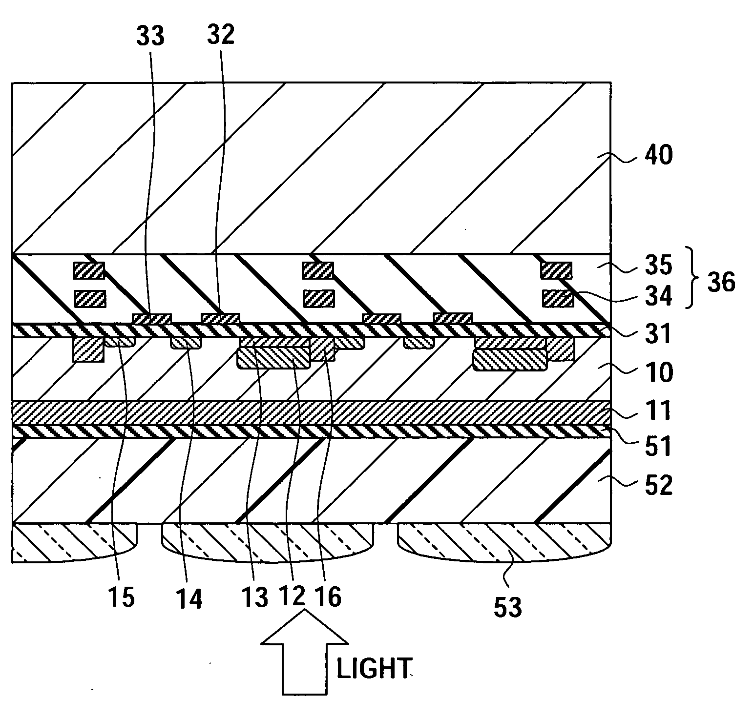
[0023]FIG. 1 is a cross-sectional view of a solid-state imaging device according to the present embodiment. In the present embodiment, a MOS type solid-state imaging device referred to a CMOS image sensor will be described.

[0024] In the present embodiment, a p-type epitaxial layer 10 of silicon is used as a substrate. The thickness of the p-type epitaxial layer 10 depends on a kind and application of the solid-state imaging device, and is preferably 4 to 6 m for visible light or 6 to 10 μm for near-infrared radiation. Further, a p-type impurity concentration (a first impurity concentration) of the p-type epitaxial layer 10 a...


PUM


Abstract

To provide a back-illuminated solid-state imaging device able to suppress a crystal defect caused by a metal contamination in a process and to suppress a dark current to improve quantum efficiency, a camera including the same and a method of producing the same, having the steps of forming a structure including a substrate, a first conductive type epitaxial layer and a first conductive type impurity layer, the first conductive type epitaxial layer being formed on the substrate to have a first impurity concentration, and the first conductive type impurity layer being formed in a boundary region to have a second impurity concentration higher than the first impurity concentration of the epitaxial layer; forming a second conductive type region storing a charge generated by a photoelectric conversion in the epitaxial layer; forming an interconnection layer on the epitaxial layer; and removing the substrate.

Description

CROSS REFERENCES TO RELATED APPLICATIONS [0001] The present invention contains subject matter related to Japanese Patent Application No. JP 2004-193278 filed in the Japanese Patent Office on Jun. 30, 2004, the entire contents of which being incorporated herein by reference. BACKGROUND OF THE INVENTION [0002] 1. Field of the Invention [0003] The present invention relates to a back illumination type (back-illuminated) solid-state imaging device receiving light from an opposite side to a surface formed with an interconnection layer, a camera including the same and a method of producing the same. [0004] 2. Description of the Related Art [0005] In recent year, in terms of an improvement of an aperture ratio for receiving light and an improvement of a flexibility of a layout of an interconnection layer, a back-illuminated solid-state imaging device in which a semiconductor layer is formed on its surface side with the interconnection layer and illuminated with light from a back surface sid...

Claims


Application Information

Patent Timeline
IPC IPC(8): H01L31/00H01L27/146H01L31/10H04N5/335H04N5/361H04N5/369
CPCH01L21/26506H01L21/3221H01L27/14632H01L27/14698H01L27/14643H01L27/14687H01L27/1464H01L27/146
Inventor KANBE, HIDEO
Owner SONY CORP
Why Eureka
Try Eureka