Method of forming MOS transistor having fully silicided metal gate electrode

a metal gate electrode and metal oxide technology, applied in the direction of semiconductor devices, basic electric elements, electrical equipment, etc., can solve the problems of reducing the transistor size, affecting the current driving capability of the transistor, and affecting the transmission speed of an electrical signal applied to the gate electrod

Inactive Publication Date: 2006-01-12
SAMSUNG ELECTRONICS CO LTD
View PDF3 Cites 17 Cited by
  • Summary
  • Abstract
  • Description
  • Claims
  • Application Information

AI Technical Summary

Benefits of technology

[0019] Embodiments of the invention provide a method of fabricating a MOS transistor which is capable of preventing a deep silicide layer from being formed in source and drain regions while a gate electrode is fully transformed to silicide.
[0027] The selective etching process may be carried out as an in-situ process. That is, it is preferable to perform the selective etching process and the selective epitaxial growth process continuously using the same apparatus. The selective etching process may be carried out using HCl and H2 gases as reaction gases and may be carried out under conditions of 700° C. to 1000° C. in temperature and 10 torr to 600 torr in pressure. The selective etching process may allow the temperature, the pressure, and the reaction gases to be adjusted to thereby change an etch selectivity between the single-crystalline semiconductor layer and the poly-crystalline semiconductor layer. The gate-reduced pattern and the elevated source and drain regions may have respective desired thicknesses by means of the etch selectivity between the single-crystalline semiconductor layer and the poly-crystalline semiconductor layer. In this case, it is preferable to form the elevated source and source regions to be protruded from the surface of the semiconductor substrate.
[0033] It is preferable to perform the selective etching process and the selective epitaxial growth process in the same apparatus. The selective etching process may be carried out using a chemical vapor deposition (CVD) apparatus. The selective etching process may be carried out using HCl and H2 gases as reaction gases and may be carried out under conditions of 700° C. to 1000° C. in temperature and 10 torr to 600 torr in pressure. The selective etching process may allow the temperature, the pressure, and the reaction gases to be adjusted to thereby change an etch selectivity between the single-crystalline semiconductor layer and the poly-crystalline semiconductor layer.

Problems solved by technology

However, the reduction of the transistor size has several associated difficulties.
In this case, the transmission speed of an electrical signal applied to the gate electrode is delayed due to a resistance-capacitance (RC) delay time.
The increase of the sheet resistance in turn causes the current driving capability of the transistor to be degraded.
In the prior art of employing polysilicon for the gate electrode, the reduction of the gate electrode size further raises problems such as polysilicon depletion and boron penetration.
However, when a thin gate insulating layer is used, the decrease in effective gate voltage due to the polysilicon depletion is raised as a serious problem.
However, the metal gate causes the gate insulating layer to be degraded due to metal ions, and its work function is constant, which makes it difficult to adjust the threshold voltage Vth.
Consequently, a metal gate employed for the N-MOS transistor region should be different from that employed for the P-MOS transistor region, which makes the process very complicated.
When the thickness of the source / drain metal silicide layer is larger than the source and drain junction depth, leakage current occurs.
Nevertheless, it is not easy to remove the capping layer 90.
For example, when the capping layer 90 is an oxide layer, a trench isolation layer which is to be concurrently exposed may be damaged.
Alternatively, when the capping layer 90 is a nitride layer, a trench liner which is to be concurrently exposed may be damaged.

Method used


Image

  • Method of forming MOS transistor having fully silicided metal gate electrode
  • Method of forming MOS transistor having fully silicided metal gate electrode
  • Method of forming MOS transistor having fully silicided metal gate electrode

Examples


Embodiment Construction

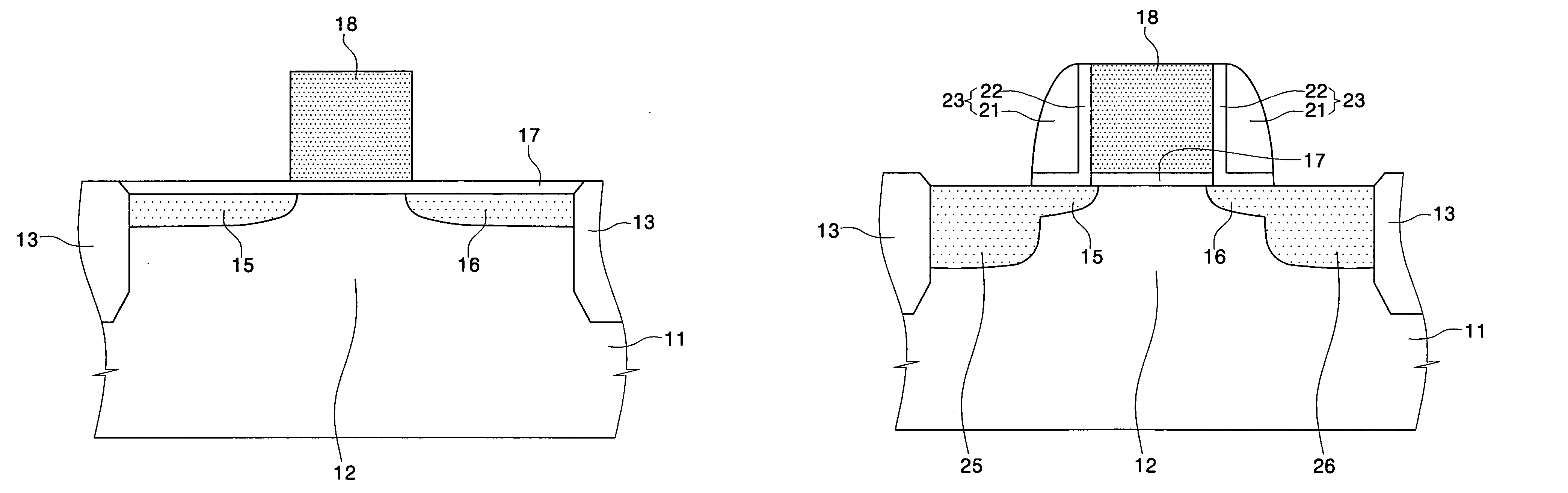
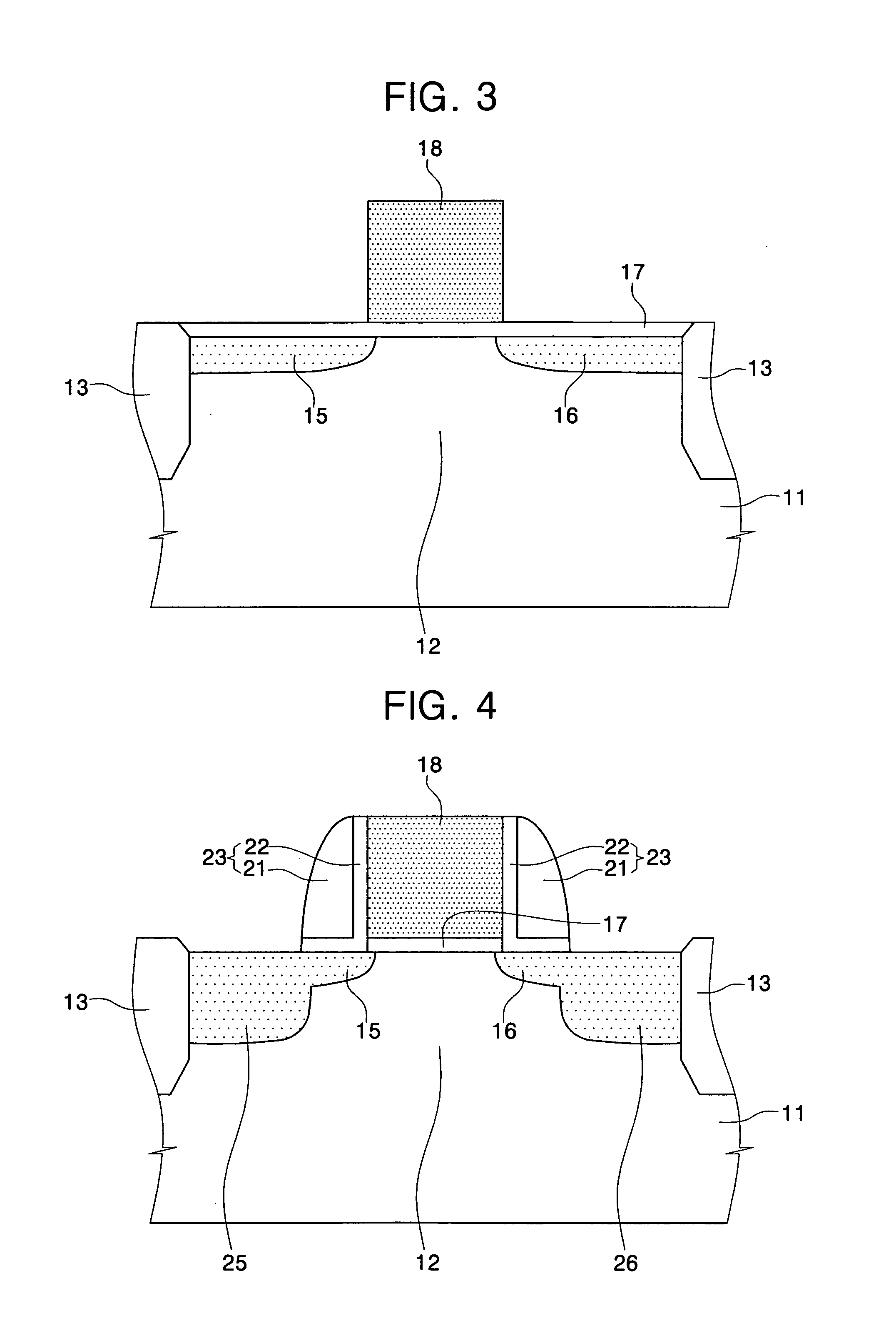
[0040]FIG. 3 to FIG. 8 are cross-sectional views illustrating a method of fabricating a MOS transistor having a fully silicided metal gate electrode in accordance with embodiments of the present invention.

[0041] Referring to FIG. 3, an isolation layer 13 is formed in a predetermined region of a semiconductor substrate 11 to define an active region 12. The semiconductor substrate 11 may be a silicon substrate or a silicon-on-insulator (SOI) substrate. Moreover, the semiconductor substrate 11 may be a strained silicon substrate containing germanium (Ge) or carbon (C). A gate insulating layer 17 is formed on the active region 12. A gate conductive layer is formed on the entire surface of the semiconductor substrate having the gate insulating layer 17. The gate conductive layer may be formed of a poly-crystalline semiconductor layer which is doped with N type impurities or P type impurities.

[0042] The gate conductive layer is patterned to form a gate pattern 18 which crosses over the ...


PUM


Abstract

Methods of fabricating a MOS transistor having a fully silicided metal gate electrode are provided. The method includes forming an isolation layer in a predetermined region of a semiconductor substrate to define an active region. An insulated gate pattern which crosses over the active region is formed. A spacer is formed on sidewalls of the gate pattern. A selective epitaxial growth process is applied to form semiconductor layers on the gate pattern and on the active region at both sides of the gate pattern. In this case, a poly-crystalline semiconductor layer is formed on the gate pattern while single-crystalline semiconductor layers are concurrently formed on the active region at both sides of the gate pattern. The semiconductor layers are selectively etched to form a gate-reduced pattern and elevated source and drain regions. Respective desired thicknesses of the gate-reduced pattern and the elevated source and drain regions may be obtained using an etch selectivity between the poly-crystalline semiconductor layer and the single-crystalline semiconductor layer. A silicidation process is applied to the semiconductor substrate where the gate-reduced pattern is formed to simultaneously form a fully silicided metal gate electrode and elevated source and drain silicide layers.

Description

CROSS-REFERENCE TO RELATED APPLICATION [0001] This application claims the benefit of Korean Patent Application No. 2004-0054160, filed Jul. 12, 2004, the contents of which are hereby incorporated herein by reference in their entirety. BACKGROUND OF THE INVENTION [0002] 1. Field of the Invention [0003] The present invention relates to a method of fabricating a semiconductor device and, more particularly, to a method of fabricating a metal oxide semiconductor (MOS) transistor having a fully silicided metal gate electrode. [0004] 2. Description of the Related Art [0005] As electronic products employing semiconductor devices require light weight and small size, high integration density per unit area, low threshold voltage Vth, fast operating speed and low power consumption. Discrete devices such as MOS transistors are widely employed as switching devices for the semiconductor devices. To meet the requirement of the high integration, a gate of a transistor, source and drain junctions of ...

Claims


Application Information

Patent Timeline
Patent Type & Authority Applications(United States)
IPC IPC(8): H01L21/336H01L21/8234
CPCH01L21/28097H01L21/823835H01L21/823842H01L29/4975H01L29/66636H01L29/6653H01L29/66545H01L29/6656H01L29/66628H01L29/665H01L21/18
Inventor LEE, SEUNG-HWANSHIN, DONG-SUKRHEE, HWA-SUNGUENO, TETSUJILEE, HO
Owner SAMSUNG ELECTRONICS CO LTD
Why Eureka
Try Eureka