Optimized plating process for multilayer printed circuit boards having edge connectors

a technology of printed circuit boards and edge connectors, which is applied in the direction of printed circuits, electrical devices, printed circuit aspects, etc., can solve the problems of not only toxic free cyanide, but also attacks photo-resistants, and self-limited reaction that does not allow thicker gold layers

Inactive Publication Date: 2006-01-12
IBM CORP
View PDF6 Cites 29 Cited by
  • Summary
  • Abstract
  • Description
  • Claims
  • Application Information

AI Technical Summary

Problems solved by technology

However, even if it is possible to build “universal” pads that support multiple electrical connection practices, the pads of some applications have to deal with constraints that are outside the specifications of such “universal” pads.
It is well known that soft gold and hard gold plating processes are not compatible in materials and processes, either in the sequence of the operations i.e., which of the two plating processes has to come last, or to the process steps that need to be performed on the two different plated portions later in the product assembly phases, due in particular to the contamination residues left from the other plating process.
However, the free cyanide is not only toxic but also attacks photo-resists used to delineate the fine pitch circuit features and wire bonding pads.
This is a self-limited reaction that does not allow thicker gold layers to grow and it is porous in nature.
The beveling step can be performed on large features (connectors' tabs) but is very

Method used


Image

  • Optimized plating process for multilayer printed circuit boards having edge connectors
  • Optimized plating process for multilayer printed circuit boards having edge connectors
  • Optimized plating process for multilayer printed circuit boards having edge connectors

Examples


Embodiment Construction

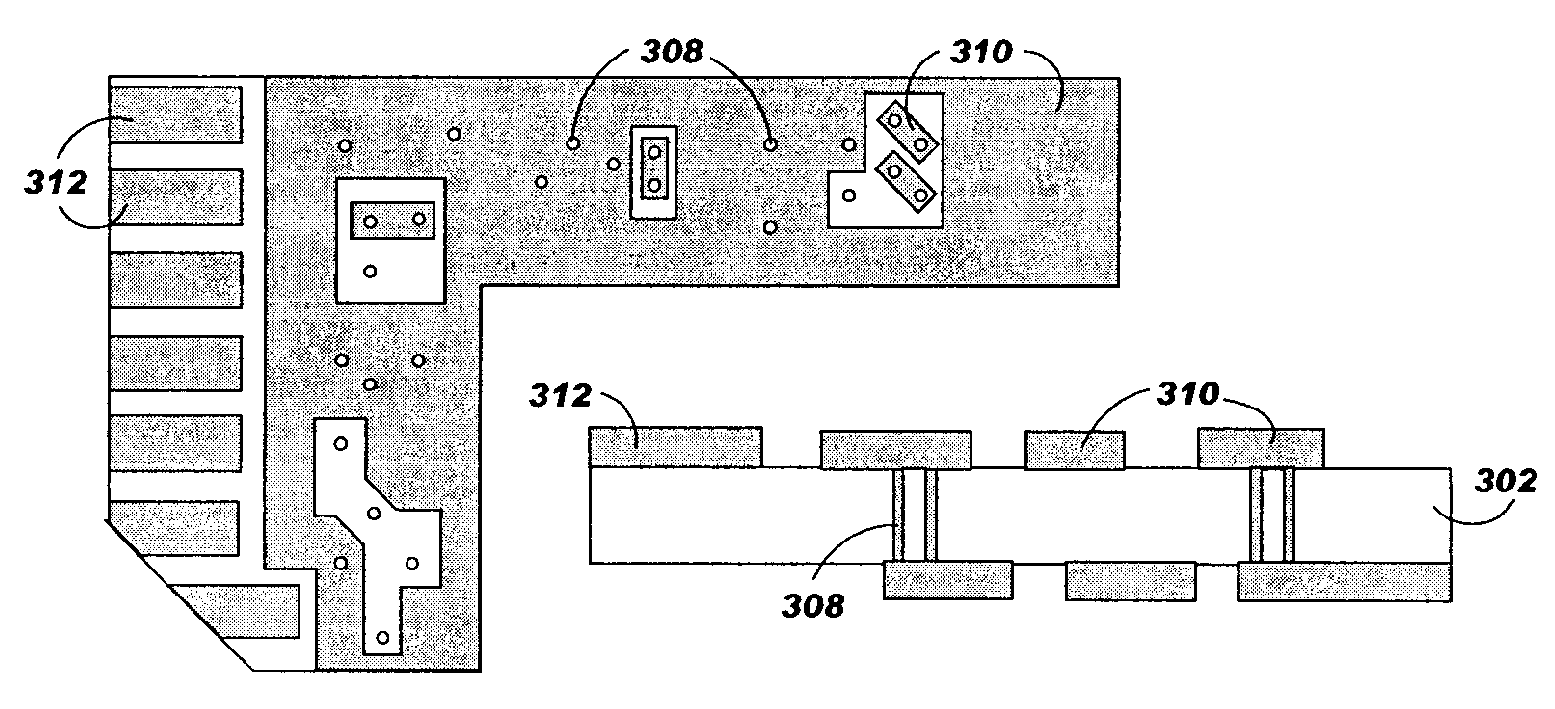
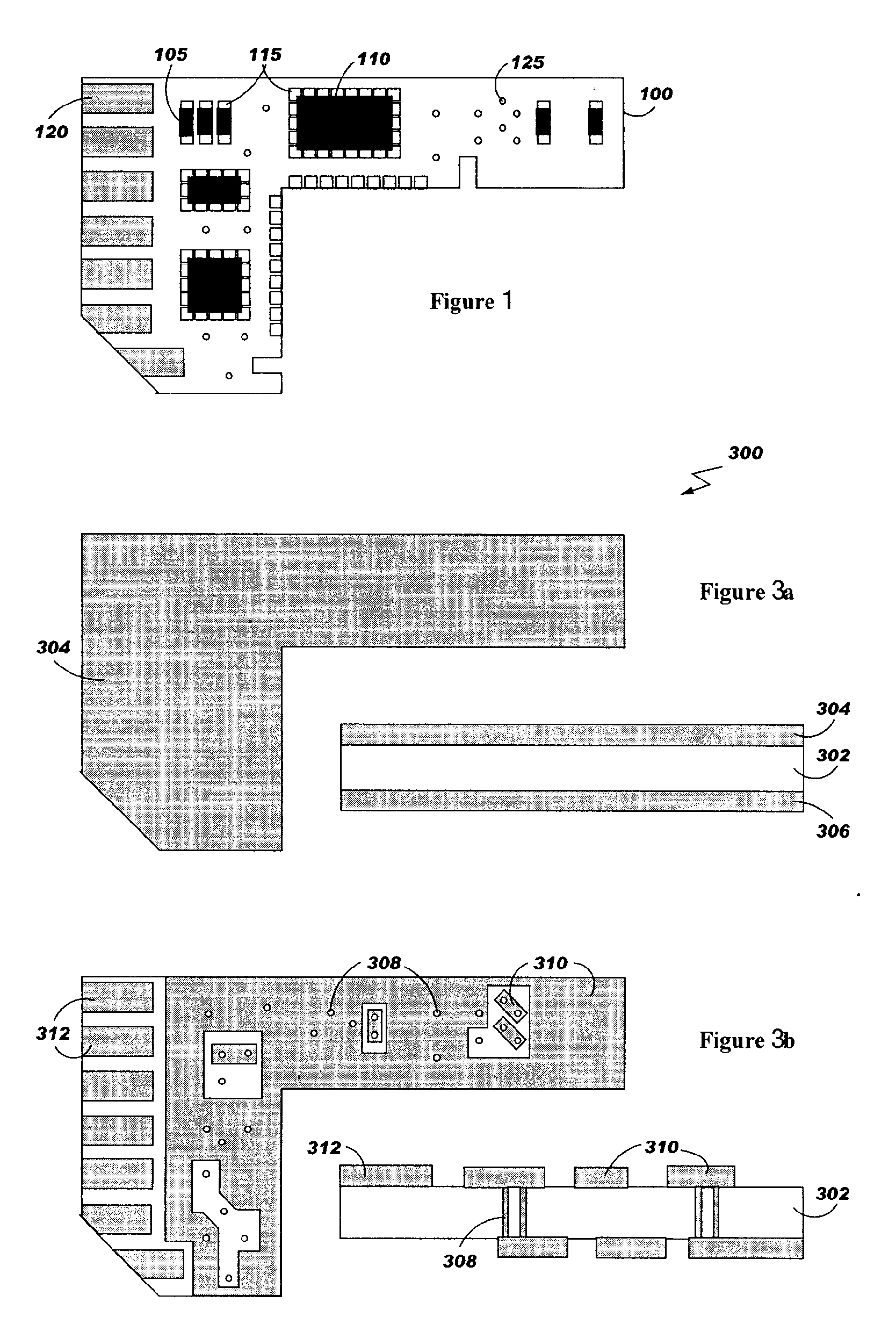
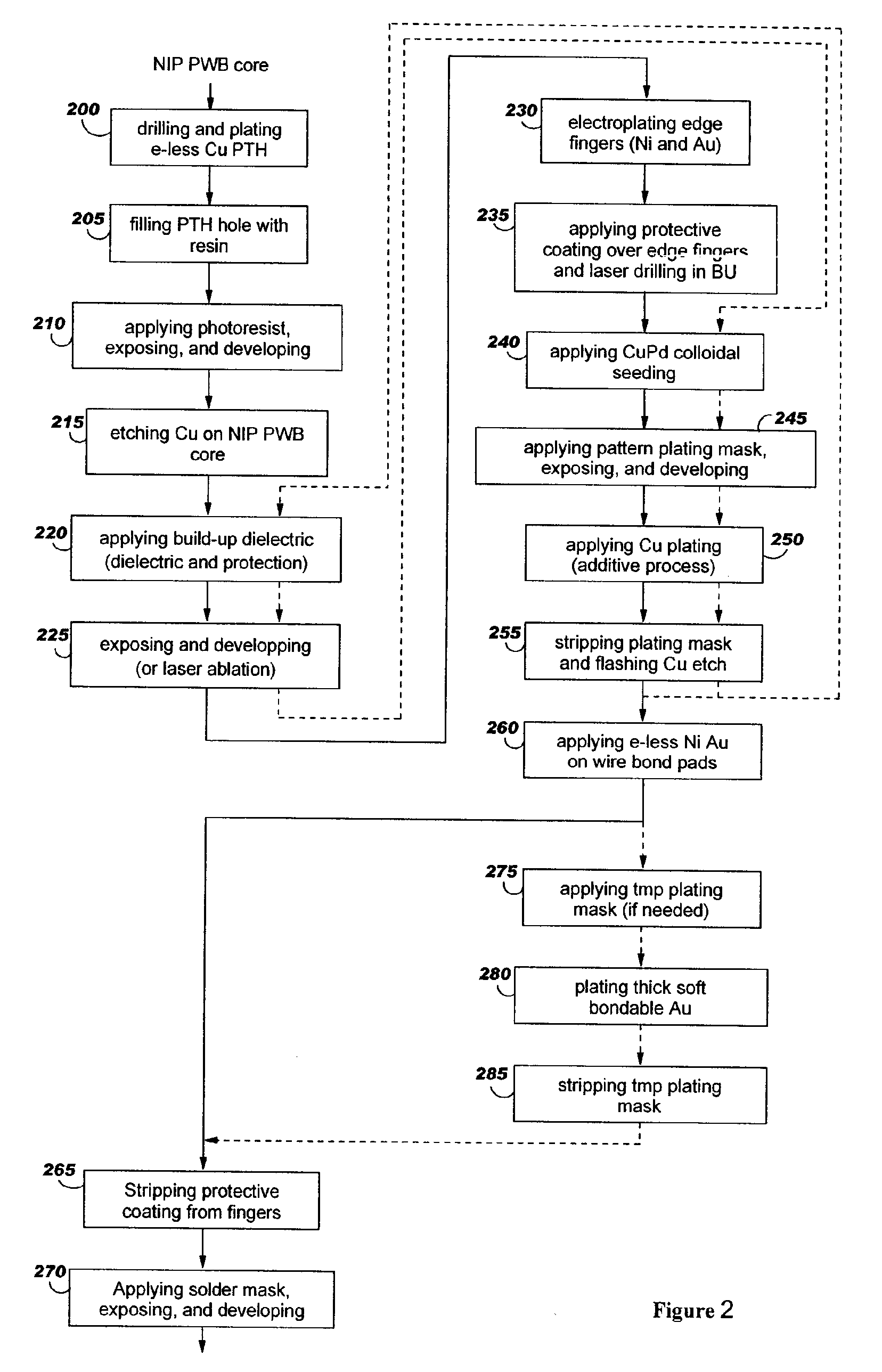
[0033] In the following detailed description of embodiments, reference is made to the accompanying drawings which form a part hereof, and in which are shown by way of illustration specific embodiments are described in sufficient detail to enable those skilled in the art to practice the invention, and it to be understood that other embodiments may be utilized and logical, structural, electrical and other changes may be made without departing from the scope of the present invention.

[0034] According to the invention there is provided a process for manufacturing printed circuit boards with hard plated sliding contact tabs and soft plated pads, using standard manufacturing steps so as to take advantage of existing manufacturing tools. For sake of illustration, the manufacturing process according to the method of the invention is described in conjunction with reinforced glass core and hard and soft gold plating however, it is to be understood that other materials can be used. For example...


PUM


Abstract

A process for manufacturing printed wire boards with hard plated sliding contact tabs and soft plated wire bond pads. Sliding contact tabs are covered by a protective coating after being hard plated thus allowing the soft plating of wire bond pads without damaging the hard plated sliding contact tabs. In a preferred embodiment, the hard plating includes the step of electroplating nickel on the sliding contact tabs, followed by electroplating an alloy of gold and cobalt, using standard electroplating process. An electro-less soft plating process includes the steps of plating a nickel layer on the wire bond pads and then a gold layer after having “flash-etched” the copper seeding.

Description

FIELD OF THE INVENTION [0001] The present invention relates generally to the manufacturing process of printed circuit boards and more specifically to an optimized process for multilayer printed circuit boards having edge connectors. BACKGROUND OF THE INVENTION [0002] A conventional printed circuit device, such as a Printed Circuit Board (PCB), also known as Printed Wire Board (PWB), includes pads for attachment of surface mounted devices and connection to other circuit elements. The surfaces are masked and the exposed pads prepared with appropriate coatings for the attachment process. Where multiple attachment techniques are used, the preparatory coatings of the pads must be adapted to the particular [0003] connective process employed. [0004] Several types of attachments require pad coatings with different physical characteristics. The application described in this document, as an example of a device employing multiple attachment techniques, is a PCB that carries wirebond chips and ...

Claims


Application Information

Patent Timeline
IPC IPC(8): H01L21/8238
CPCH05K1/117H05K3/243H05K3/244H05K2203/0723H05K2203/054H05K2203/058H05K2203/072H05K2201/0391
Inventor OGGIONI, STEFANOVIERO, GIORGIO
Owner IBM CORP
Why Eureka
Try Eureka