Semiconductor device with crack prevention ring and method of manufacture thereof

a technology of crack prevention and semiconductor devices, which is applied in the direction of semiconductor devices, semiconductor/solid-state device details, electrical apparatus, etc., can solve the problems of increasing the complexity of manufacturing processes, increasing the functional complexity of integrated circuits, and challenging various aspects of multi-level interconnect processes, so as to prevent cracking and improve device yield , the effect of high mechanical strength

Active Publication Date: 2006-01-19
TAIWAN SEMICON MFG CO LTD
View PDF6 Cites 129 Cited by
  • Summary
  • Abstract
  • Description
  • Claims
  • Application Information

AI Technical Summary

Benefits of technology

[0012] An advantage of embodiments of the present invention includes providing a method of forming a crack prevention ring at the edges of an integrated circuit die that prevents cracking and delaminating of the dielectric material of the integrated circuit during the separating of the die into individual die. The crack prevention ring comprises a conductive material which has a high mechanical strength and is robust. The conductive material of the crack prevention ring is formed perpendicular to the crack direction / wafer direction, thereby providing structural support for the edges of the integrated circuit die during the singulation process. The crack prevention ring may be formed while test pads of the integrated circuit are being formed, for example, in the scribe line region. Device yields are improved, resulting in a cost savings.

Problems solved by technology

Scaling or reducing the size increases circuit performance, primarily by increasing circuit speed, and also increases the functional complexity of the integrated circuits.
Implementing a multilevel interconnect process to a fabrication scheme increases the complexity of the manufacturing process.
As semiconductor devices continue to shrink, various aspects of multilevel interconnect processes are challenged.
The propagation delay of integrated circuits becomes limited by the large RC time delay of interconnection lines when minimum feature size is decreased below about 1 μm, for example.
In particular, the change in the conductive materials and insulating materials used in multilevel interconnect schemes is proving challenging and requires a change in a number of processing parameters.
Along with these advancements, the challenges of maintaining yield and throughput have also increased.
Low-k materials tend to be weaker and less robust than the silicon dioxide that was used as a dielectric material in the past.
As far as reliability is concerned, the low-k material near die corners has a tendency to crack / delamination, especially in the sawing process to separate the die from one another.
Consequently, portions of the wafer around the scribe line suffer damage, such as peeling, delamination, or dielectric fracture.
The stress resulting from the sawing process causes serious peeling starting from near the test keys at the die corners.
This results in delamination at the interface between the multiple layers at the die corners.
Delamination impacts the reliability of the device, and contributes to production of stringers (residual materials) that interfere with further processing and testing of the integrated circuit.
If a low-k material is used near the guard ring corners, the crack issue becomes more serious and further reduces reliability.

Method used


Image

  • Semiconductor device with crack prevention ring and method of manufacture thereof
  • Semiconductor device with crack prevention ring and method of manufacture thereof
  • Semiconductor device with crack prevention ring and method of manufacture thereof

Examples


Embodiment Construction

[0020] The making and using of the presently preferred embodiments are discussed in detail below. It should be appreciated, however, that the present invention provides many applicable inventive concepts that can be embodied in a wide variety of specific contexts. The specific embodiments discussed are merely illustrative of specific ways to make and use the invention, and do not limit the scope of the invention.

[0021] The present invention will be described with respect to preferred embodiments in a specific context, namely a semiconductor device having low dielectric constant materials as insulating layers. Embodiments of the invention may also be applied, however, to other semiconductor devices comprising more traditional dielectric materials and ultra-low dielectric constant materials, as examples.

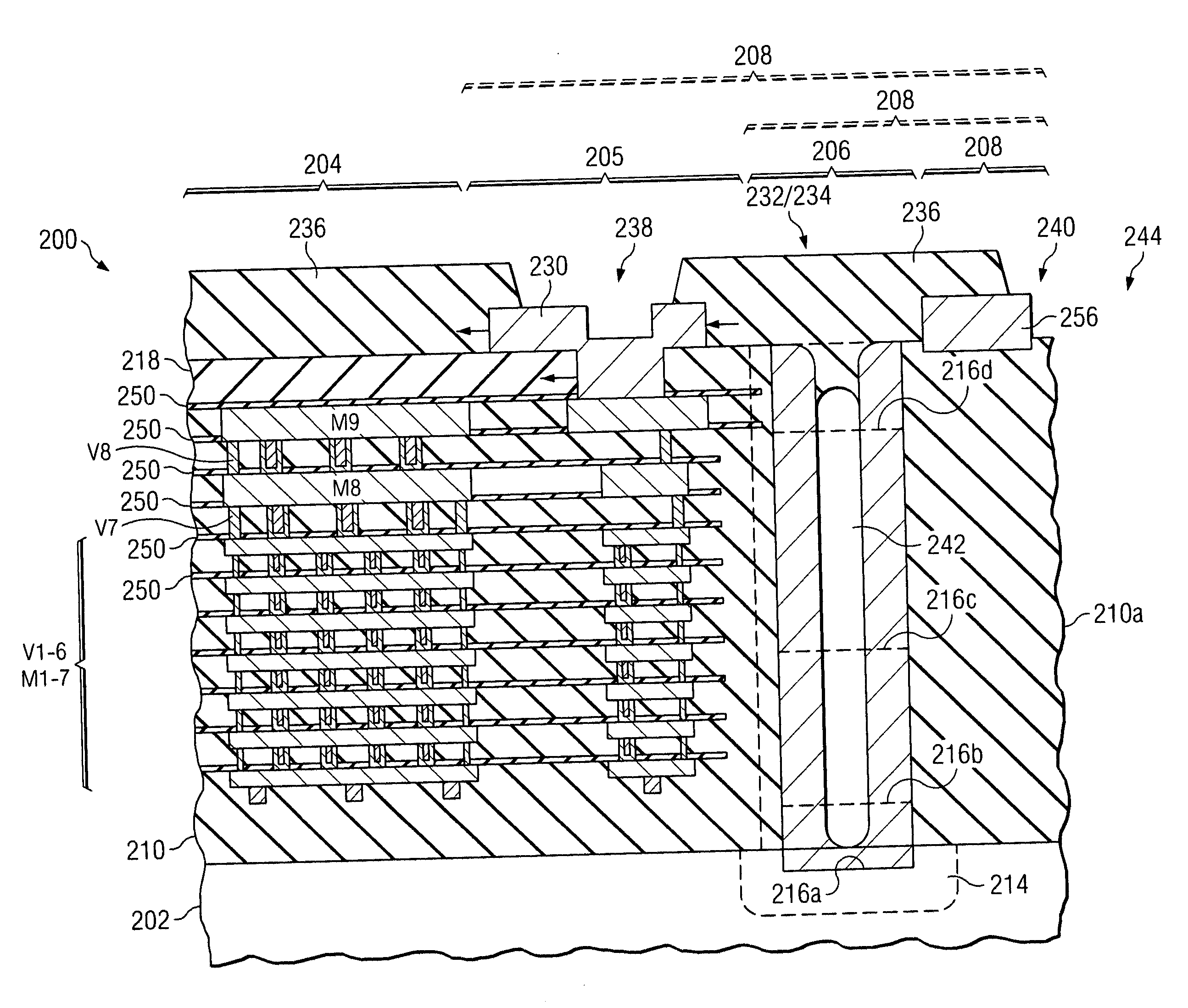
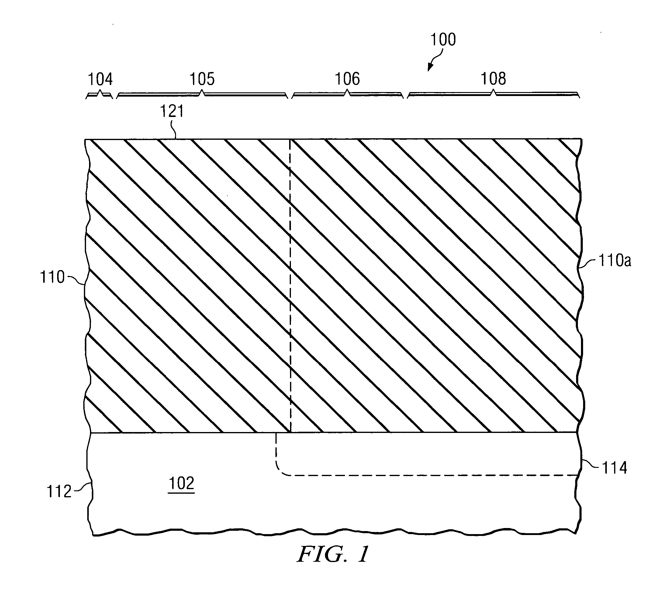
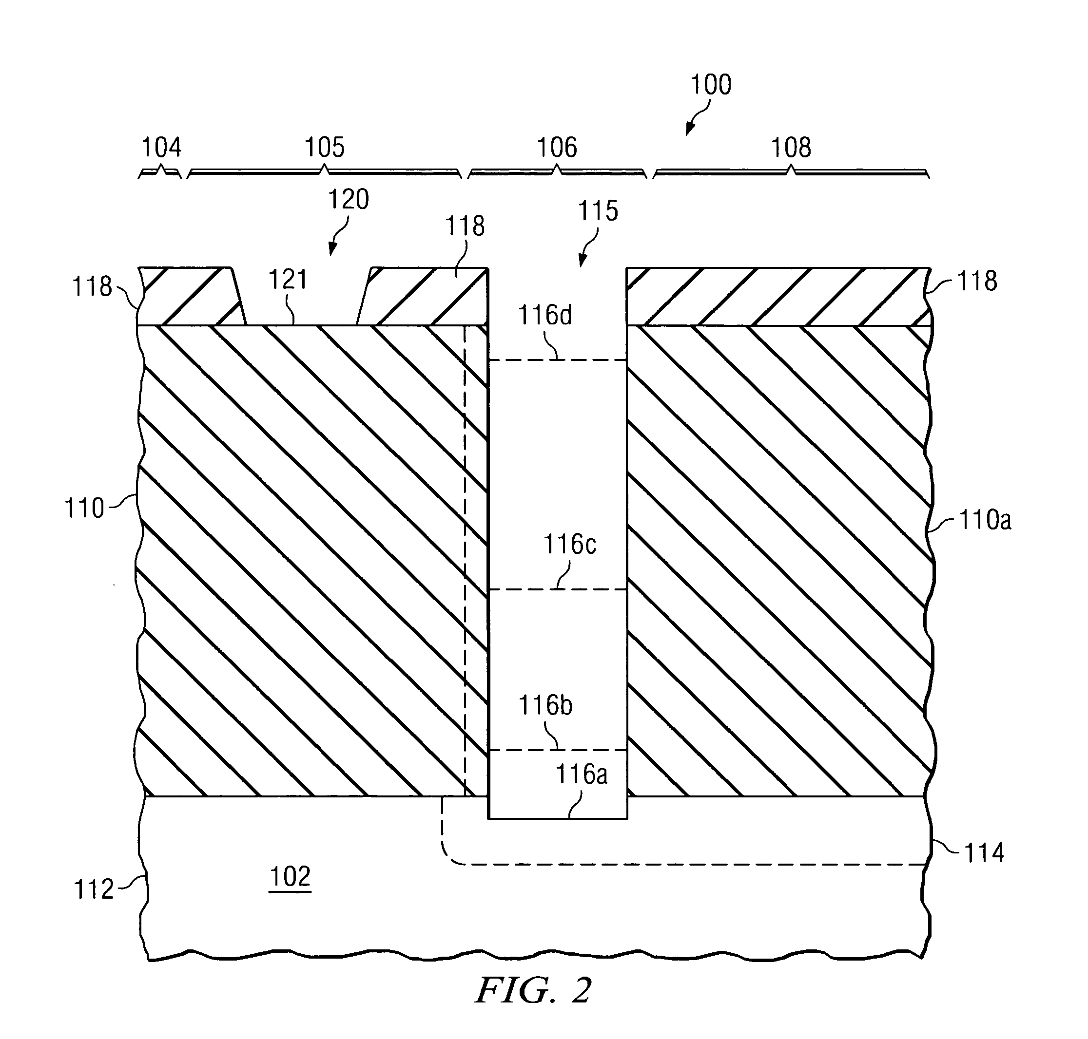
[0022]FIGS. 1 through 5 and 6a show cross-sectional views of a semiconductor device at various stages of manufacturing in accordance with an embodiment of the present invention. Refe...


PUM


Abstract

A method of forming a crack prevention ring at the exterior edge of an integrated circuit to prevent delamination and cracking during the separation of the integrated circuits into individual die. The crack prevention ring extends vertically into a semiconductor workpiece to at least a metallization layer of the integrated circuit. The crack prevention ring may be formed simultaneously with the formation of test pads of the integrated circuits. The crack prevention ring may be partially or completely filled with conductive material. An air pocket may be formed within the crack prevention ring beneath a passivation layer of the integrated circuit. The crack prevention ring may be removed during the singulation process. An optional seal ring may be formed between the crack prevention ring and the integrated circuit.

Description

TECHNICAL FIELD [0001] The present invention relates generally to semiconductor devices, and more particularly to the formation of a seal ring at the edge of an integrated circuit to prevent delamination and cracks in insulating layers of the integrated circuit during die separation. BACKGROUND [0002] In the evolution of integrated circuits in semiconductor technology, there has been a trend towards device scaling. Scaling or reducing the size increases circuit performance, primarily by increasing circuit speed, and also increases the functional complexity of the integrated circuits. The number of devices per integrated circuit (also referred to in the art as a chip or die) has increased throughout the years. When integrated circuits contained only a small number of devices per chip, the devices could be easily interconnected in a single level. However, the need to accommodate more devices and increased circuit speed has led to the use of multi-level or multi-layer interconnects. [0...

Claims


Application Information

Patent Timeline
Patent Type & Authority Applications(United States)
IPC IPC(8): H01L23/544
CPCH01L23/562H01L23/585H01L23/60H01L2924/0002H01L2924/00
Inventor WANG, PING-WEIWU, CHII-MING MORRIS
Owner TAIWAN SEMICON MFG CO LTD
Why Eureka
Try Eureka