Nanodots formed on silicon oxide and method of manufacturing the same

a technology of silicon oxide and nanodots, which is applied in the field of nanodots formed on silicon oxide, can solve the problems of difficult to form nanodots having a uniform size and distribution, conventional methods that do not allow for forming nanodots having uniformity, and methods that are not easily adapted to the practical manufacture of semiconductor devices

Active Publication Date: 2006-01-19
SAMSUNG ELECTRONICS CO LTD
View PDF13 Cites 28 Cited by
  • Summary
  • Abstract
  • Description
  • Claims
  • Application Information

AI Technical Summary

Benefits of technology

[0021] The locations corresponding to the metal dots may be locations proximate to the metal dots and may correspond to regions of the silicon oxide layer that have a surface stress that is higher than a surface stress for regions of the silicon oxide layer that are peripheral to the metal dots.
[0022] The

Problems solved by technology

Accordingly, using conventional methods, it may be difficult to form nanodots having a uniform size and distribution.
Conventional methods do not allow for forming nanodots having uniform sizes equal to or smaller than 10 nanometers (nm) on

Method used


Image

  • Nanodots formed on silicon oxide and method of manufacturing the same
  • Nanodots formed on silicon oxide and method of manufacturing the same
  • Nanodots formed on silicon oxide and method of manufacturing the same

Examples


experimental example

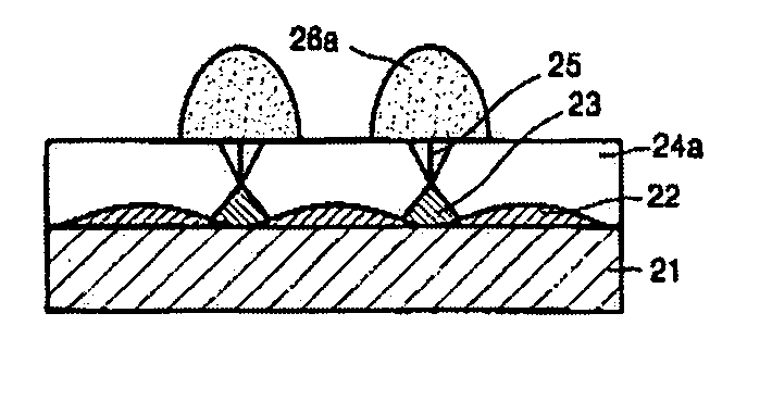
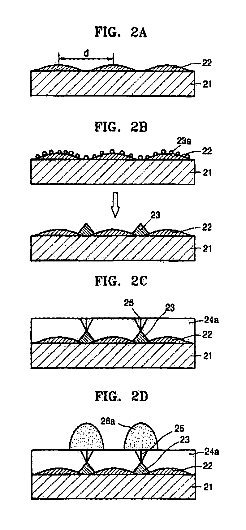
[0039] A silicon (111) substrate was provided and an uneven surface with a periodicity of about 2.7 nm was formed on the surface. A 0.35 nm monolayer of Al was deposited on the silicon substrate at about 575° C. to form regularly arranged Al nanodots on the silicon substrate.

[0040] Next, a silicon oxide layer having a thickness of about 4 nm was deposited on the silicon substrate and the Al nanodots using inductively couple plasma CVD (ICP-CVD). The deposition temperature was about 400° C., silane (SiH4) and nitrous oxide (N2O) were used as material gasses and mixed with each other, and helium was used as a buffer gas.

[0041] Alternatively, to oxidize the surface of the silicon substrate and not separately deposit an oxide layer, oxygen plasma or a thermal oxidation processes may be employed. For the oxygen plasma process, electron cyclotron resonance (ECR) plasma may be used to generate high-density plasma, including a microwave output of 1000 W and plasma in which a N2O gas and h...


PUM


Abstract

A nanodot material including nanodots formed on silicon oxide, and a method of manufacturing the same, is provided. The nanodot material includes a substrate, a silicon oxide layer, and a plurality of nanodots on the silicon oxide layer.

Description

BACKGROUND OF THE INVENTION [0001] 1. Field of the Invention [0002] The present invention relates to nanodots formed on silicon oxide and a method of manufacturing the same. More particularly, the present invention relates to nanodots whose location can be controlled so that the nanodots are regularly arranged on the silicon oxide. [0003] 2. Description of the Related Art [0004] Nanodots may be used in a wide variety of optical devices including, e.g., light emitting diodes (LEDs), laser diodes (LDs) and photodetectors. Nanodots may also be used in, e.g., single electron transistors, etc. Though the use of nanodots, it may be possible improve the performance of a device by, e.g., reducing a threshold current of the device, improving retention characteristics, increasing an optical gain, etc. [0005] As an example, when a plurality of nanodots are distributed throughout a floating gate of a flash memory device, the current required for storing information may be smaller than the curre...

Claims


Application Information

Patent Timeline
IPC IPC(8): H01L21/8232B82Y10/00B82Y40/00H01L21/20H01L21/336H01L21/8247H01L27/115H01L29/06H01L29/788H01L29/792
CPCB82Y10/00H01L21/28273B82Y20/00Y10S977/742Y10S977/777H01L29/40114
Inventor PARK, YOUNG-SOOPARK, WAN-JUNSARANIN, ALEXANDER ALEXANDROVICHZOTOV, ANDREY VADIMOVICH
Owner SAMSUNG ELECTRONICS CO LTD
Why Eureka
Try Eureka