

Charged particle beam exposure apparatus, charged particle beam exposure method and device manufacturing method
- Summary
- Abstract
- Description
- Claims
- Application Information
AI Technical Summary
Benefits of technology
Problems solved by technology
Method used
Image

Examples
first embodiment
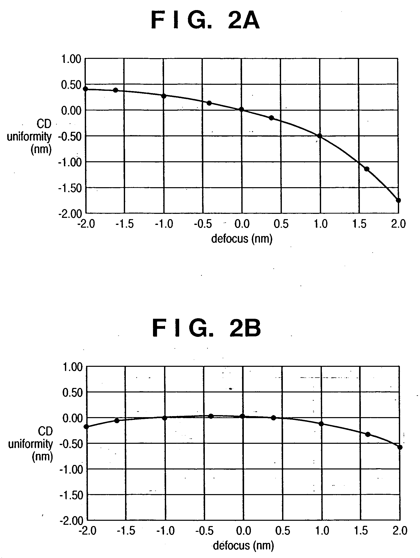
(1) An Electron Beam Exposure Apparatus Which Performs Blanking in a Direction Vertical to a Raster Scanning Direction
[0035] In this apparatus, the drawing-pattern dimensional accuracy can be improved by blanking an electron beam in a direction vertical to a raster scanning direction.
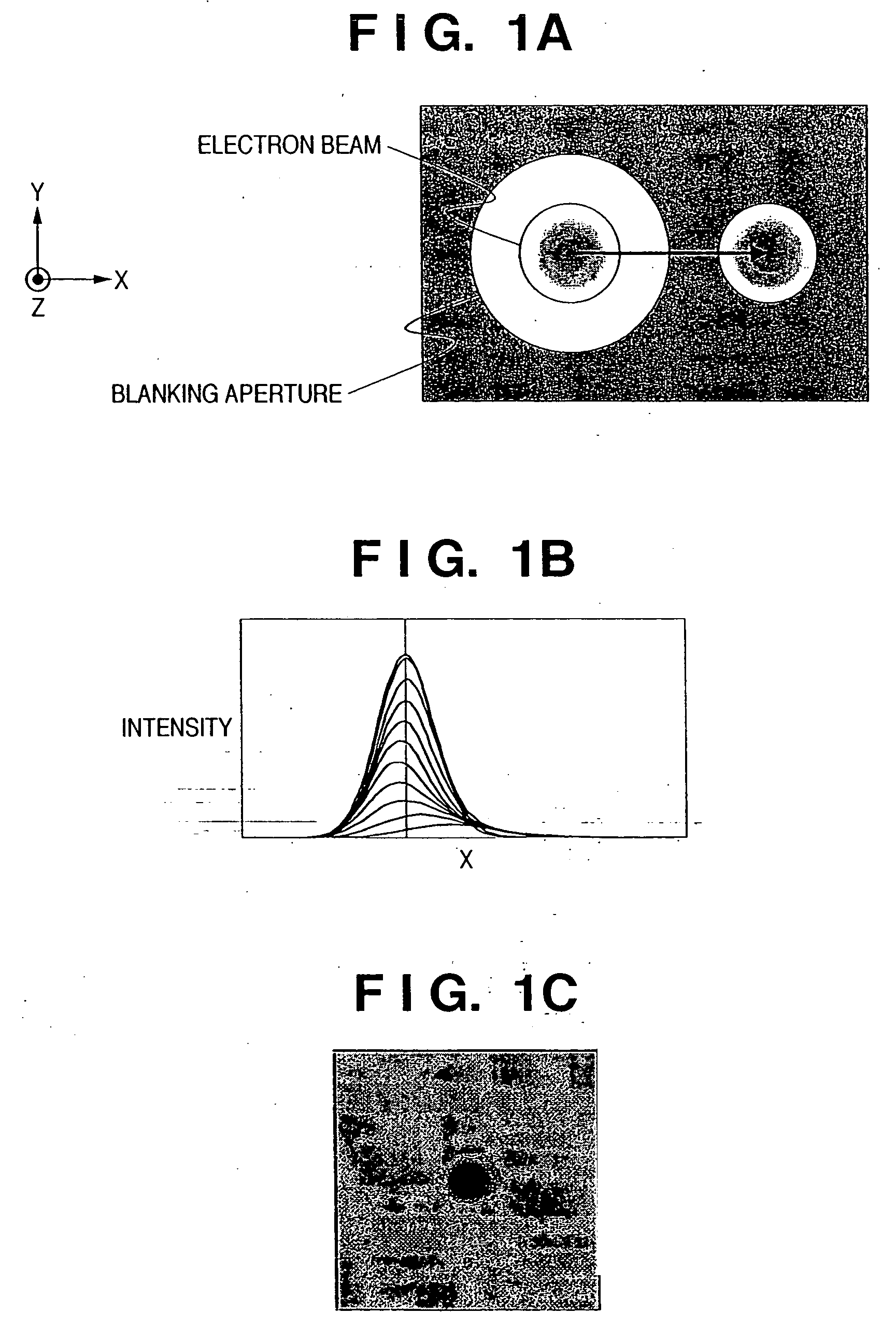
[0036] First, the spreading of the electron beam current intensity distribution in a blanking direction will be described with reference to FIGS. 1A to 1C.
[0037] As shown in FIG. 1A, the blanking operation is changing a status where an electron beam is passing through a blanking aperture without actuating a blanker to a status where the blanker is actuated to move the electron beam in a direction X and the electron beam is blocked by the blanking aperture. At this time, the electron beam moves in the direction X in predetermined transition time. As shown in FIG. 1B, the beam current intensity distribution on a wafer is the moving average of the electron beam when it is blocked by the blanking apertu...
second embodiment
(2) Electron Beam Exposure Apparatus Which Performs Blanking in a Direction Where a Beam Diameter is the Shortest (Single Electron Beam is Used)
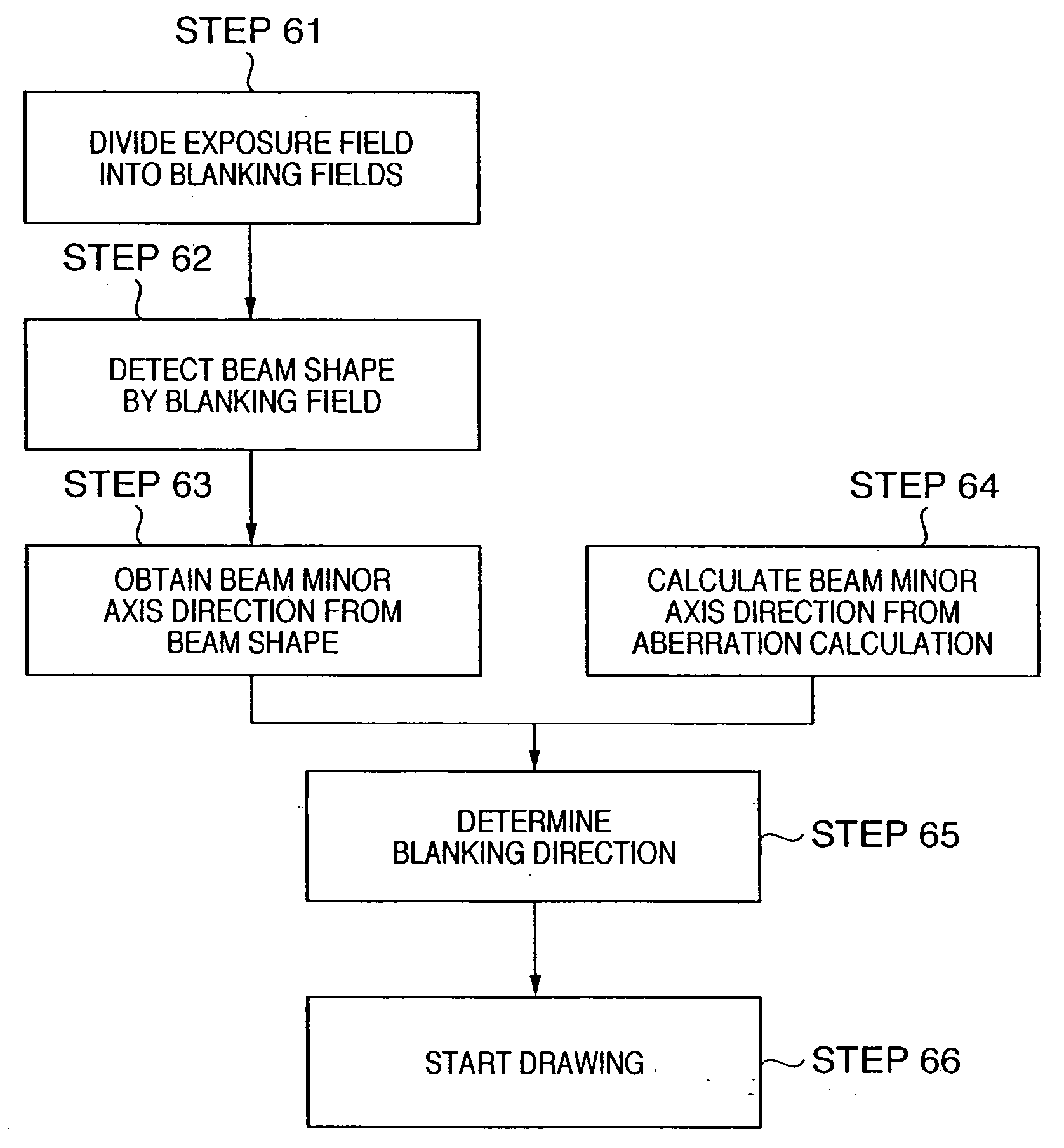
[0045] Next, the operation of the electron beam exposure apparatus according to the present embodiment will be described with reference to FIG. 3.
(Step 61)
[0046] As shown in FIG. 4, an exposure field 701 in a substrate to be exposed by using the electron beam is divided into blanking fields 702 as plural small areas. In FIG. 4, the exposure field is divided into 4×4 blanking fields. In the present embodiment, the blanking direction is set by blanking field. The number of divided blanking fields is not limited to that of this example. Further, the shape of blanking field is not limited to square. When the exposure field 701 has been divided into the blanking fields 702, the process proceeds to Step 62.
(Step 62)
[0047] In each blanking field 702, the beam shape is detected in the central position or maximum deflection position. When the...
third embodiment
(3) Electron Beam Exposure Apparatus Which Performs Blanking in a Direction Where a Beam Diameter is the Shortest (Plural Electron Beams are Used)
[0057]FIG. 6 is a substantial-part schematic cross-sectional view of a multi-beam type electron-beam exposure apparatus according to a third embodiment of the present invention.
[0058] Numerals 901 to 909 denote multisource modules which form plural electron source images and emit electron beams from the electron source images. In FIG. 6, 5×5 (25) multisource modules are arranged in two-dimensional array. Numeral 901 denotes an electron source (crossover image) formed by electron guns. An electron beam emitted from the electron source 901 becomes an approximately collimated electron beam via a condenser lens 902. Numeral 903 denotes an aperture array formed with a two-dimensional array of apertures; 904, a lens array formed with a two-dimensional array of electrostatic lenses having the same optical power; 905 to 908, multi deflector arr...
PUM
 Abstract
Description
Claims
Application Information