Semiconductor device with high-k gate dielectric and quasi-metal gate, and method of forming thereof

a semiconductor and dielectric technology, applied in the field of semiconductor device manufacturing, can solve the problems of short channel effect, less desirable commercial devices using high-k dielectric materials, and inability to manufacture reliable mos transistors

Active Publication Date: 2006-01-26
TAIWAN SEMICON MFG CO LTD
View PDF34 Cites 69 Cited by
  • Summary
  • Abstract
  • Description
  • Claims
  • Application Information

AI Technical Summary

Benefits of technology

[0010] Various embodiments of the present invention provide a novel process and structure for a planar MOS transistor using a high-k gate dielectric material and a doped gated electrode material.
[0015] Embodiments of the invention avoid too large a threshold voltage for PMOS with n+ doped poly gate and for NMOS with p+ doped poly gate. A net concentration of n-type poly dopants in PMOS is preferably at least two times smaller than a net concentration of n-type dopants in NMOS. Such a doping reduces the threshold voltage for PMOS with an n+ doped poly gate. For the same reason, a net concentration of p-type poly dopants in NMOS is preferably at least two times smaller than a net concentration of p-type dopants in PMOS.
[0017] Preferred embodiments of the invention advantageously limit poly gate depletion. Such advantages achieve thinner EOT and higher performance such as are normally achieved with metal gates. In this way, desired metal gate properties are achieved in embodiments of the invention.

Problems solved by technology

Reduced device scaling with conventional gate dielectrics creates problems in manufacturing reliable MOS transistors, including short channel effects (SCE).
The use of such materials creates additional problems, however, in the manufacturing and reliability of the transistor devices, including a threshold voltage (Vt) variability in the MOS transistors, particularly of p-type MOS transistors, which makes commercial devices using the high-k dielectric materials less desirable.
Further, reduction in scale and the use of certain desirable high-k dielectric materials on silicon substrates is believed to contribute to a reported degradation in carrier mobility, which has a negative effect on the performance of transistors manufactured using these materials.

Method used


Image

  • Semiconductor device with high-k gate dielectric and quasi-metal gate, and method of forming thereof
  • Semiconductor device with high-k gate dielectric and quasi-metal gate, and method of forming thereof
  • Semiconductor device with high-k gate dielectric and quasi-metal gate, and method of forming thereof

Examples


Embodiment Construction

[0027] The operation and fabrication of the presently preferred embodiments are discussed in detail below. However, the embodiments and examples described herein are not the only applications or uses contemplated for the invention. The specific embodiments discussed are merely illustrative of specific ways to make and use the invention, and do not limit the scope of the invention or the appended claims.

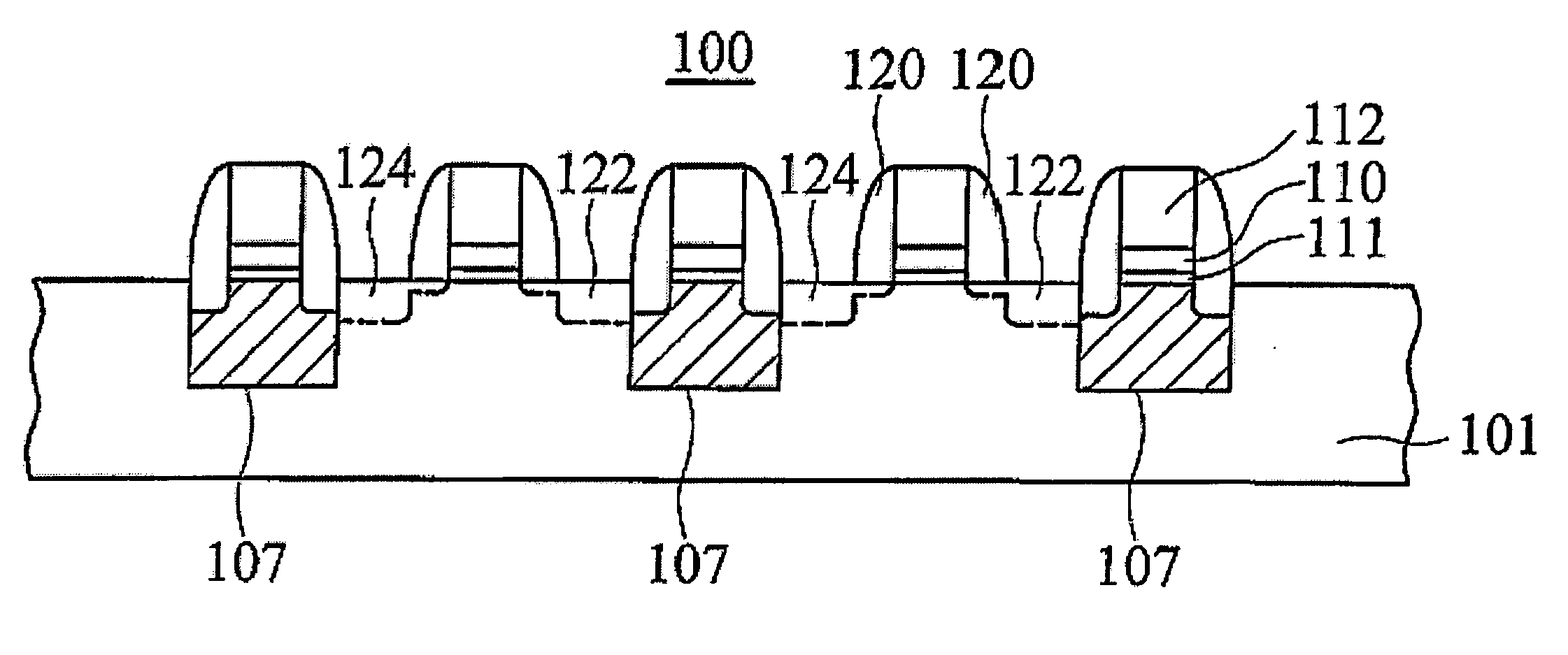
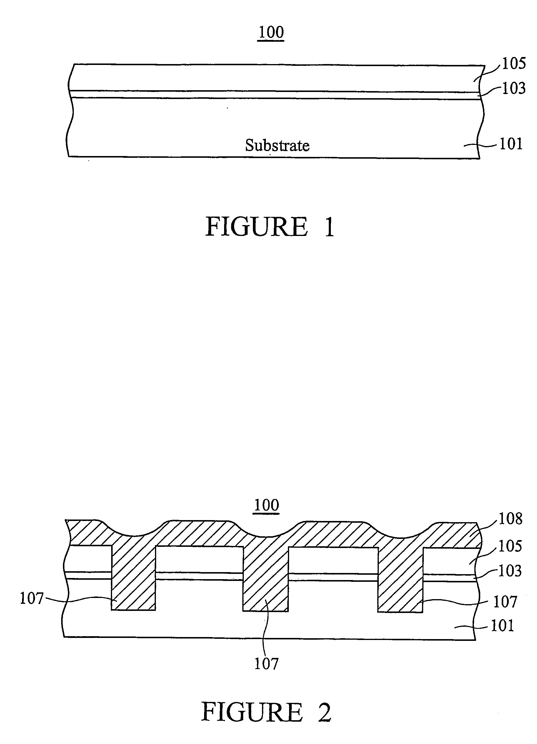
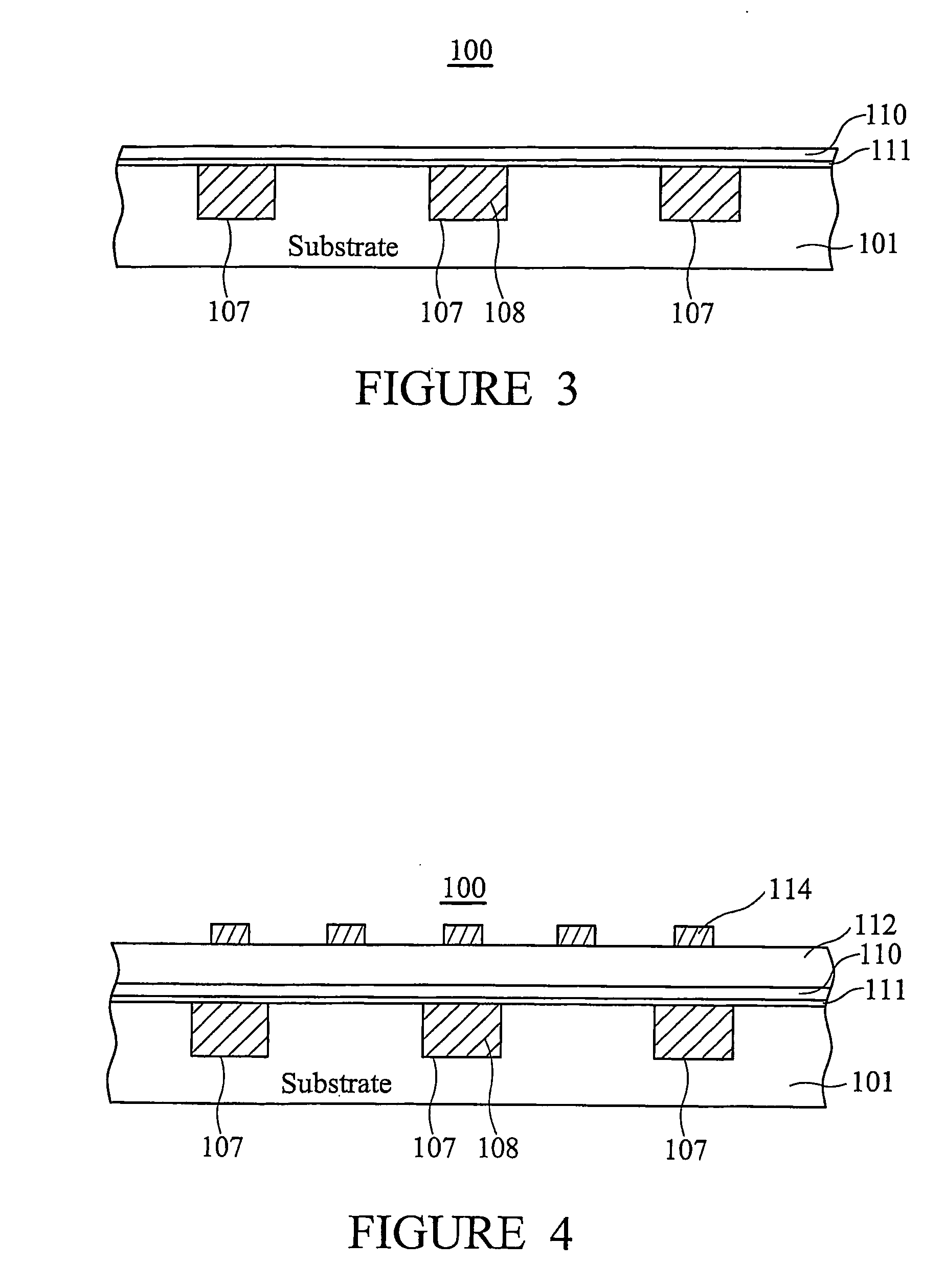
[0028]FIG. 1 depicts a cross sectional view of a semiconductor device 100 not drawn to scale, but drawn as an illustration only. Semiconductor substrate 101 will provide the basic material for the manufacture of the device. The semiconductor substrate 101 includes silicon, germanium, strained silicon, strained germanium, silicon germanium or SOI substrate, or their combination substrate. Silicon substrate can be epitaxial silicon on silicon and SOI. Germanium substrate includes epitaxial silicon germanium on silicon. The substrate 101 is shown with a pad oxide layer 103 and a nitride...


PUM


Abstract

A process and apparatus for a semiconductor device is provided. A device comprises a first transistor having a first charge carrier type. The first transistor comprises a high-k gate dielectric and a first doped electrode. The first charge carrier type comprises one of p-type and n-type and the first doped electrode comprises the other of p-type and n-type. The device further comprises a second transistor having a charge carrier type opposite the first charge carrier type. The second transistor comprises the high-k gate dielectric, and a second doped electrode, wherein the second doped electrode comprises the other of p-type and n-type.

Description

[0001] This application claims the benefit of U.S. Provisional Application No. 60 / 590,060, filed on Jul. 21, 2004, entitled “Semiconductor Device with High-k Gate Dielectric and Quasi Metal Gate,” which application is hereby incorporated herein by reference.TECHNICAL FIELD [0002] This invention and the various embodiments described generally relate to the fabrication of semiconductor devices, and more particularly to transistors having high-k gate dielectrics. BACKGROUND [0003] In the semiconductor art, it is desirable to improve transistor performance even as devices become smaller due to ongoing scaling. Reduced device scaling with conventional gate dielectrics creates problems in manufacturing reliable MOS transistors, including short channel effects (SCE). It is known in the prior art to use high-k dielectric materials as the gate dielectric material to improve device performance. For purposes of this description, a high-k dielectric is a material having a dielectric constant k ...

Claims


Application Information

Patent Timeline
Patent Type & Authority Applications(United States)
IPC IPC(8): H01L29/94H01L29/76
CPCH01L21/28123H01L21/28194H01L29/7833H01L29/517H01L29/518H01L21/28202
Inventor WANG, CHIH-HAOTSAI, CHING-WEIHU, CHENMING
Owner TAIWAN SEMICON MFG CO LTD
Why Eureka
Try Eureka