Low thermal budget silicon nitride formation for advance transistor fabrication

a technology of silicon nitride and silicon nitride, which is applied in the direction of chemical vapor deposition coating, solid-state devices, coatings, etc., can solve the problems of low dissociation efficiency, significant disadvantage for future applications regardless, and the damage of plasma ions in the active transistor region of the devi

Inactive Publication Date: 2006-01-26
APPLIED MATERIALS INC
View PDF67 Cites 94 Cited by
  • Summary
  • Abstract
  • Description
  • Claims
  • Application Information

AI Technical Summary

Problems solved by technology

Although, plasma enhanced-CVD (PE-CVD) processes are attractive means to deposit silicon-containing materials with low thermal budget, undesirably, the plasma ions may damage the active transistor regions of a device.
These precursors and their process regime for the advanced semiconductor device requirements, particularly for the device generation 90 nm and below, cause significant disadvantages for future applications regardless of apparatus employed.
Silane, dichlorosilane and ammonia have the fundamental limitations of low dissociation efficiency at temperatures below 600° C. due to the strong intermolecular bonds, therefore, are not production worthy precursors.
In addition, at a temperature less than 550° C., the film property may be poor and not desirable (e.g., low density and high hydrogen content) and poor performance (e.g., step coverage and micro-loading for disilane is worse than market accepted level).
High chlorine content may cause defects or particle issues to process kits and may inhibit etch selectivity, which makes the film less useful for etch stop layer application.
However, BTBAS combined with ammonia has a slow deposition rate.
For example, BTBAS / ammonia usually has a deposition rate of only a few Angstroms per minute at temperature below 550° C., which is not a production worthy process.
Conventional methods for forming silicon nitride as a sidewall structure often lead to deactivation of the semiconductor gate.
This migration causes dopant loss and subsequently, deactivation of the semiconductor gate with increased resistance of gate material.
The increase of resistivity from the metal contact due to silicide degradation will cause higher power consumption and the excessive heat generation causes premature failure of a transistor.

Method used


Image

  • Low thermal budget silicon nitride formation for advance transistor fabrication
  • Low thermal budget silicon nitride formation for advance transistor fabrication
  • Low thermal budget silicon nitride formation for advance transistor fabrication

Examples


example 1

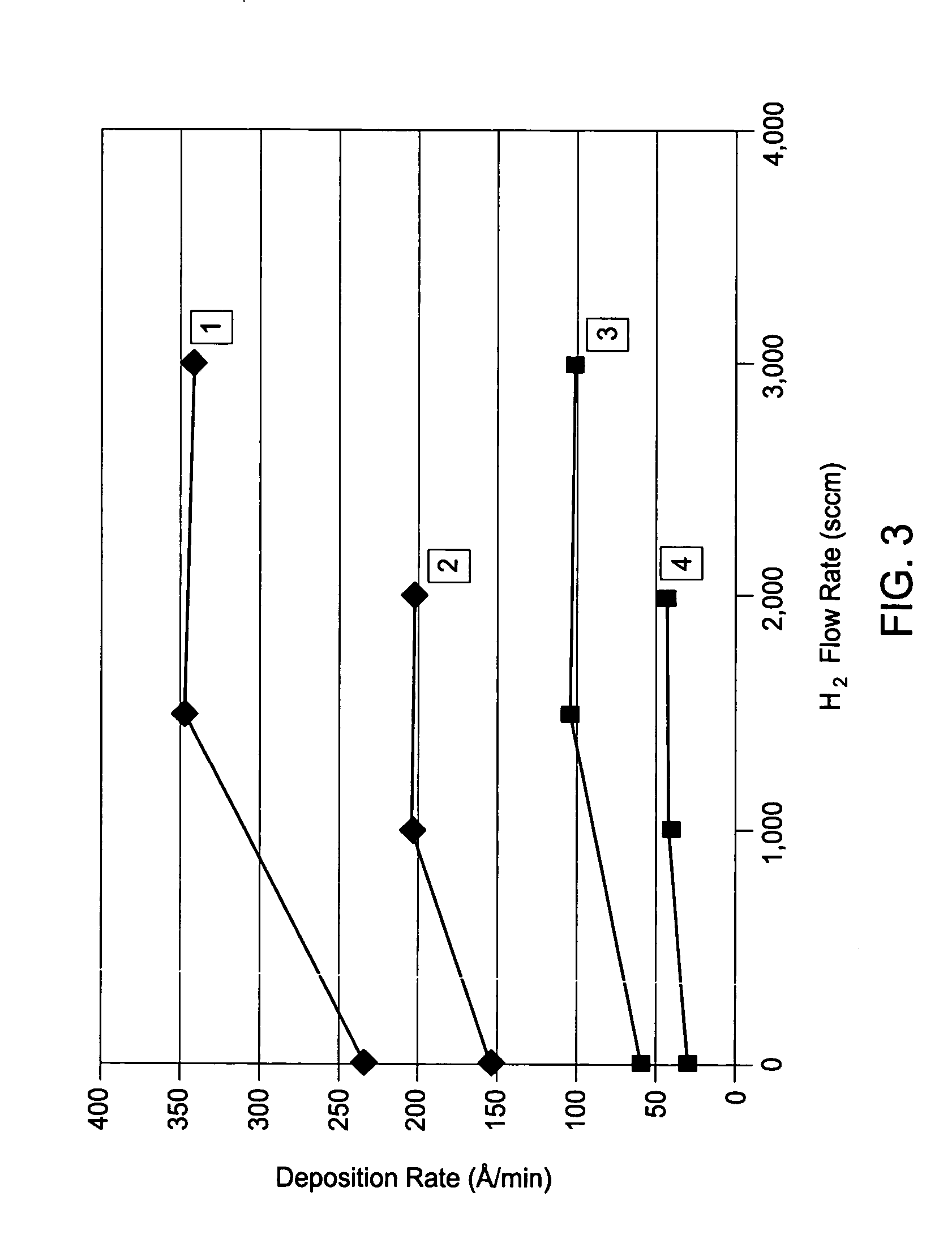
[0047] A 300 mm substrate has placed into the process chamber and maintained at about 550° C. at a pressure of about 250 Torr. A process gas containing hydrogen gas (H2) with a flow rate of about 2,000 sccm and BTBAS ((tBu(H)N)2SiH2) with a flow rate of about 50 sccm was exposed to the substrate surface. A silicon nitride material was deposited at a rate of about 60 Å / min for about 5 minutes to produce a film with a thickness about 300 Å.

example 2

[0048] A 300 mm substrate has placed into the process chamber and maintained at about 475° C. at a pressure of about 450 Torr. A process gas containing silane (SiH4) with a flow rate of about 1,000 sccm and BTBAS with a flow rate of about 30 sccm was exposed to the substrate surface. A silicon nitride material was deposited at a rate of about 50 Å / min for about 5 minutes to produce a film with a thickness about 250 Å.

example 3

[0049] A 300 mm substrate has placed into the process chamber and maintained at about 425° C. at a pressure of about 450 Torr. A process gas containing disilane (Si2H6) with a flow rate of about 1,000 sccm and BTBAS with a flow rate of about 25 sccm was exposed to the substrate surface. A silicon nitride material was deposited at a rate of about 40 Å / min for about 5 minutes to produce a film with a thickness about 200 Å.


PUM

PropertyMeasurementUnit
temperatureaaaaaaaaaa
temperaturesaaaaaaaaaa
temperatureaaaaaaaaaa

Abstract

In one embodiment, a method for depositing a layer containing silicon nitride on a substrate surface is provided which includes positioning a substrate in a process chamber, maintaining the substrate at a predetermined temperature, and exposing the substrate surface to an alkylaminosilane compound and at least one ammonia-free reactant. In another embodiment, a method for depositing a silicon nitride material on a substrate is provided which includes positioning a substrate in a process chamber, maintaining the substrate at a predetermined temperature, and exposing the substrate surface to bis(tertiarybutylamino)silane and a reagent, such as hydrogen, silane and / or disilane.

Description

BACKGROUND OF THE INVENTION [0001] 1. Field of the Invention [0002] Embodiments of the invention generally relate to methods for depositing silicon-containing materials, more particularly, embodiments of the invention relate to chemical vapor deposition techniques for thermally depositing silicon nitride materials on substrate surfaces. [0003] 2. Description of the Related Art [0004] Thermal chemical vapor deposition (CVD) of silicon nitride is the state of the art, in front-end process used during semiconductor device manufacturing. In a thermal-CVD process, thermal energy is utilized for breaking the feedstock chemical, typically a silicon precursor, to make a solid thin film on the substrate surface. Alternatively, a thermal-CVD process may activate two or more precursors including the silicon precursor to generate an atomically heterogeneous silicon-containing film during the fabrication of an advanced semiconductor device. [0005] A deposition chamber equipped with a thermal sou...

Claims


Application Information

Patent Timeline
Patent Type & Authority Applications(United States)
IPC IPC(8): C23C16/00
CPCC23C16/308C23C16/345C23C16/45553H01L2924/0002H01L21/3185H01L2924/00H01L21/02211H01L21/02271H01L21/0228H01L21/0217H01L21/324
Inventor WANG, YAXINIYER, SURYANARAYANANSEUTTER, SEAN
Owner APPLIED MATERIALS INC
Why Eureka
Try Eureka