Semiconductor device with trench type device isolation layer and method for fabricating the same

a technology of semiconductor devices and trenches, which is applied in the direction of semiconductor devices, radio frequency controlled devices, electrical equipment, etc., can solve the problems of generating a lot of leakage current, reducing the effective area of source/drain regions, and the typical device isolation method such as the locos method or the pbl method has reached a limitation in the application field

Inactive Publication Date: 2006-02-02
SK HYNIX INC
View PDF8 Cites 12 Cited by
  • Summary
  • Abstract
  • Description
  • Claims
  • Application Information

AI Technical Summary

Benefits of technology

[0018] It is, therefore, an object of the present invention to provide a semiconductor device preventing a leakage current problem as a spacing distance between devices has decreased and a void generation due to a high aspect ratio and a method for fabricating the same.

Problems solved by technology

However, the LOCOS method produces a bird's beak by oxidizing lateral sides of the exposed portions of the substrate.
As a result, a width of the device isolation region gets wide, thereby decreasing an effective area of source / drain regions.
Accordingly, a crystal defect is generated on the silicon substrate, thereby generating a lot of leakage current.
Thus, the typical device isolation method such as the LOCOS method or the PBL method has reached a limitation in the application.
However, although the device isolation is carried out by using the STI process, a spacing distance S between the active regions 11A has decreased and thus, there are a lot of difficulties in controlling a leakage current problem between the devices.
Due to the aforementioned leakage current problem, refresh time of the DRAM gets shortened.
Furthermore, the conventional device isolation method cannot avoid a problem of generating a void due to a high aspect ratio during the deposition of the device isolation insulation layer 16 filled into the plurality of trenches 15.
This void may induce a defect in the polishing by stopping the polishing activity during the CMP process.
Also, there may be another problem that the void blocks the device isolation insulation layer from acting as an intended device isolation layer.

Method used


Image

  • Semiconductor device with trench type device isolation layer and method for fabricating the same
  • Semiconductor device with trench type device isolation layer and method for fabricating the same
  • Semiconductor device with trench type device isolation layer and method for fabricating the same

Examples


Embodiment Construction

[0025] Hereinafter, detailed descriptions of preferred embodiments of the present invention will be provided with reference to the accompanying drawings.

[0026] The preferred embodiment of the present invention to be explained hereinafter forms a device isolation layer as a dual structure including a first device isolation layer and a second device isolation layer as well as an active region as a dual structure including a first active region and a second active region.

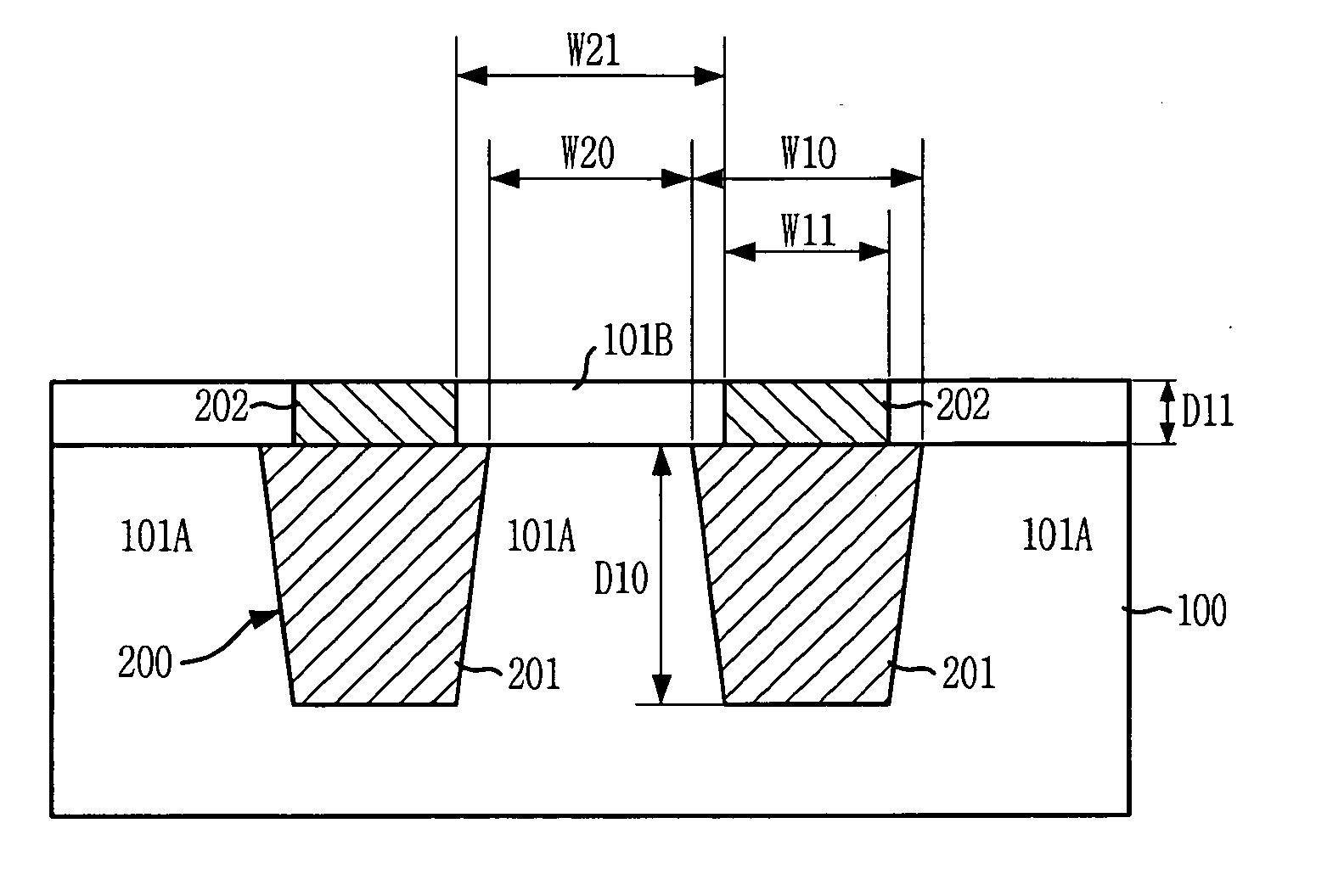
[0027]FIG. 2 is a cross-sectional view illustrating a device isolation structure of a semiconductor device in accordance with the preferred embodiment of the present invention.

[0028] As shown in FIG. 2, the device isolation structure includes: a substrate 100; a plurality of trenches 200 defining first active regions 101A each formed in a predetermined portion of the substrate 100; a plurality of first device isolation layers 201 individually filled into the plurality of trenches 200; a plurality of second device is...


PUM


Abstract

Disclosed are a semiconductor device with a device isolation structure and a method for fabricating the same. The method includes the steps of: forming a plurality of trenches defining first active regions by etching a substrate in a predetermined depth; forming a plurality of first device isolation layers in inner sides of the plurality of trenches; forming a plurality of second device isolation layers on the plurality of first device isolation layers as remaining a space opening an upper portion of each first active region disposed between the second device isolation layers; and forming a plurality of second active regions connected to the first active region between the second device isolation layers.

Description

FIELD OF THE INVENTION [0001] The present invention relates to a technology of fabricating a semiconductor device; and more particularly, to a device isolation structure of a semiconductor device and a method for fabricating the same. DESCRIPTION OF RELATED ARTS [0002] In general, a device isolation (ISO) process of a semiconductor device forms a field insulation layer in predetermined portions of a semiconductor device by using a typical device isolation method such as a local oxidation of silicon (LOCOS) method or a profiled grove isolation (PGI) method, thereby forming a field region determining an active region. [0003] Among the device isolation methods, the LOCOS method forms a nitride layer which is a mask that determines an active region on a substrate and then, exposes predetermined portions of the substrate by patterning the nitride layer through a photolithography process. Afterwards, a field oxide layer used as a device isolation region is formed by oxidizing the exposed ...

Claims


Application Information

Patent Timeline
Patent Type & Authority Applications(United States)
IPC IPC(8): H01L29/00H01L21/8238
CPCH01L21/823481H01L21/76224H01L21/76
Inventor SEO, DAE-YOUNG
Owner SK HYNIX INC
Why Eureka
Try Eureka