Method of producing a structure on the surface of a substrate

a substrate and structure technology, applied in the direction of photomechanical treatment originals, instruments, photomechanical equipment, etc., can solve the problems of limited structure resolution limit, high cost, and high cost, and achieve the effect of maintenance, and reducing the cost of production

Active Publication Date: 2006-02-02
CHANGXIN MEMORY TECH INC
View PDF7 Cites 45 Cited by
  • Summary
  • Abstract
  • Description
  • Claims
  • Application Information

AI Technical Summary

Benefits of technology

[0018] In a further preferred embodiment, the photoresist layer serving as filling material is exposed and developed in patterned fashion. In this way, it is possible to produce further structure elements on the substrate surface which, by way of example, connect the structure elements of the first and second partial structures to one another.
[0019] In this connection, it is preferred, in particular, for the first partial structure on the surface of the substrate additionally

Problems solved by technology

In this case, the resolution limit that can be achieved for the structures is primarily limited by the wavelength of the radiation used.
However, all these techniques will only be available in the future.
However, since each structure element has to be written individually in the case of this method, the method proves to be very time-intensive.
Moreover, the method is relatively expensive on account of the low throughput resulting from this.
However, possible overlay errors of the two separate lithography processes prove to be

Method used


Image

  • Method of producing a structure on the surface of a substrate
  • Method of producing a structure on the surface of a substrate
  • Method of producing a structure on the surface of a substrate

Examples


first embodiment

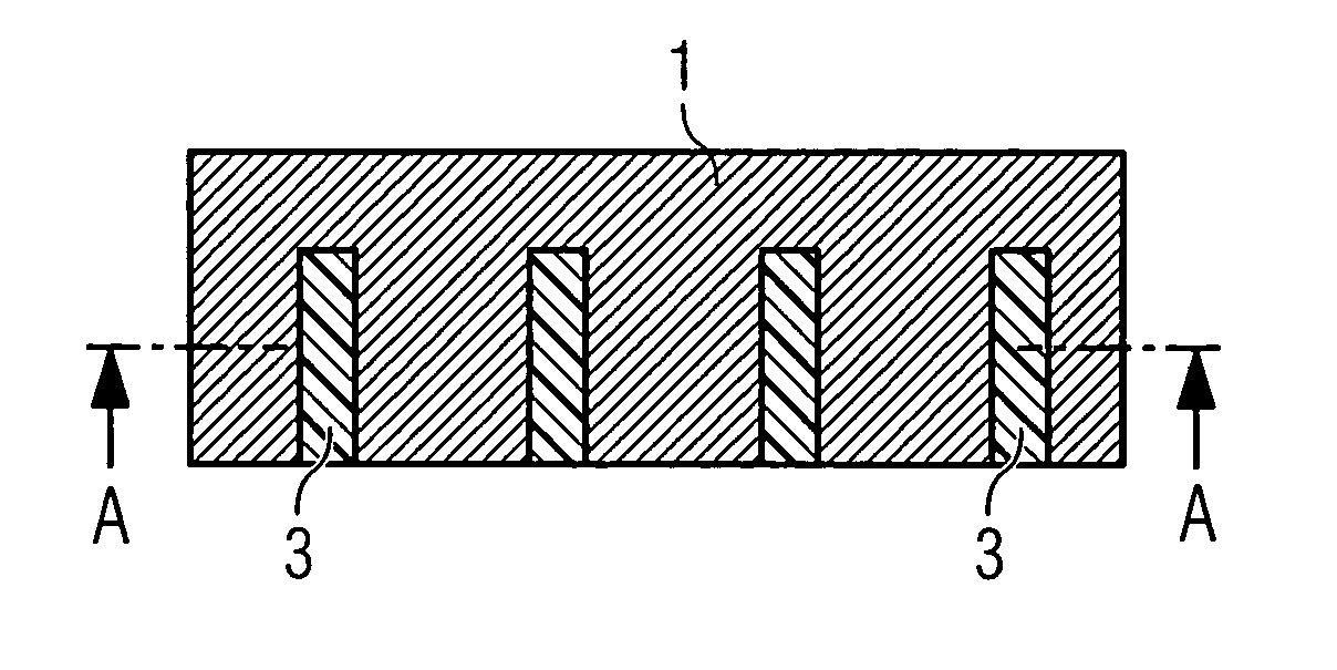
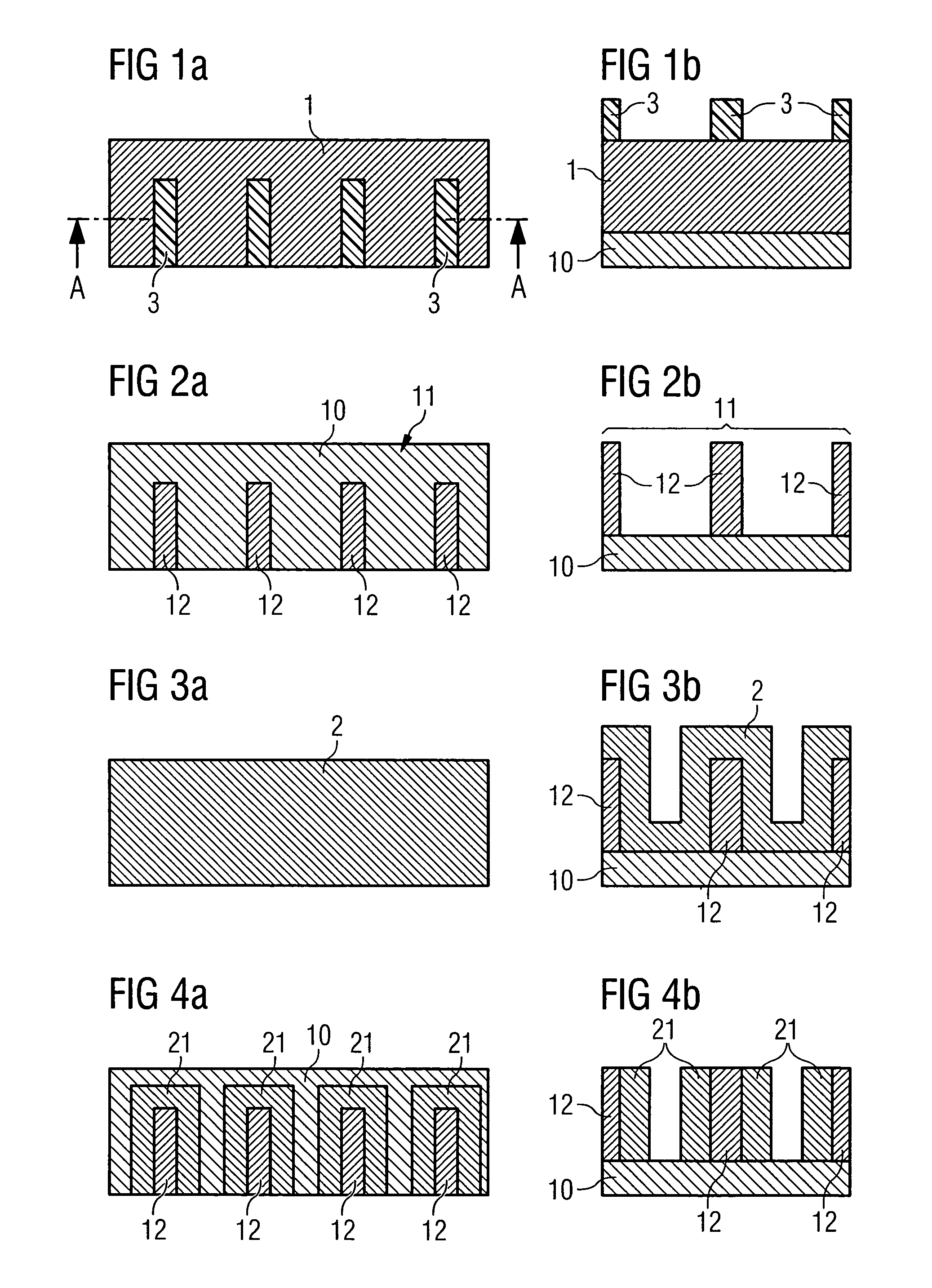
[0026]FIGS. 1a to 7a show the production of a structure serving as an etching mask on the surface of a substrate 10 in accordance with a method according to the invention in plan view. Lateral sectional illustrations corresponding to FIGS. 1a to 7a along the section line AA of FIG. 1a are shown in FIGS. 1b to 7b. In this method, a first partial structure 11 is formed on the substrate surface 10 with the aid of a customary lithography process, the partial structure having lines 12 arranged on a regular center-to-center distance grid.

[0027] For this purpose, a layer 1 is applied to the substrate surface 10 and a photoresist layer 3 is subsequently deposited onto the layer 1. Afterward, the photoresist layer 3 is patterned by means of corresponding exposure and development processes, the patterned photoresist layer 3, as illustrated in FIGS. 1a and 1b, having a regular pattern of lines that are spaced apart essentially identically. The substrate 10 is for example a silicon substrate wa...

second embodiment

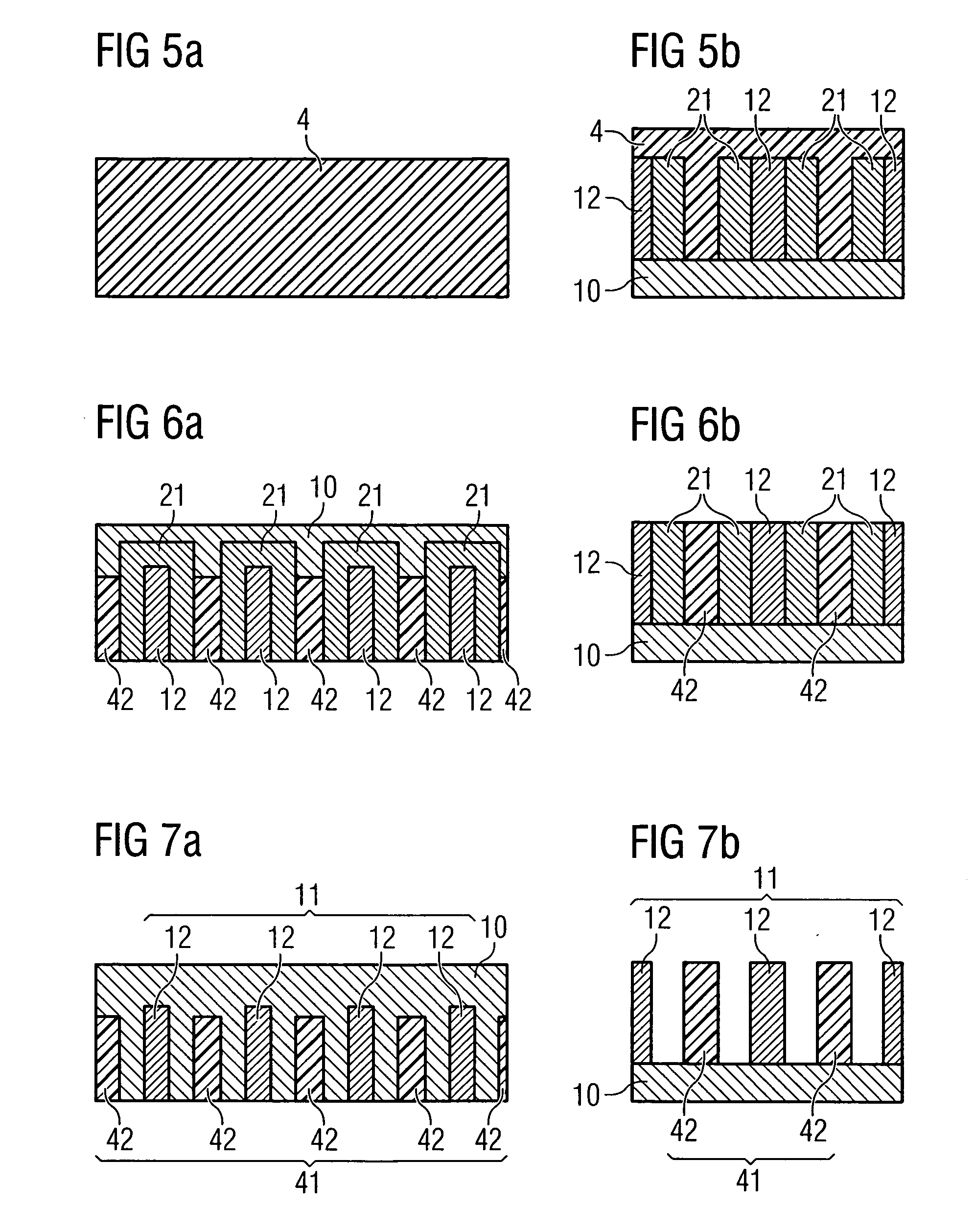
[0039] Further embodiments of a method according to the invention are conceivable for producing a structure comprised of two partial structures. In a second embodiment, after production of a first partial structure 11 comprising lines 12 that are spaced apart essentially identically on a substrate surface 10 and application of a spacer layer 2, which can be carried out in a corresponding manner in accordance with the method steps described above with reference to FIGS. 1a to 3a and 1b to 3b, an anisotropic etching of the spacer layer 2 is dispensed with. As shown in FIG. 8, firstly a filling material 4 is applied in large-area fashion to the spacer layer 2 whilst filling the cutouts provided from the spacer layer 2.

[0040] Afterward, the filling material 4 and a part of the spacer layer 2 are eroded for example with the aid of a dry etching process or a CMP method in such a way that the surfaces of the lines 12, as illustrated in FIG. 9, are uncovered and the filling material 4 remai...

third embodiment

[0043] In contrast to the methods described above, a photoresist is used as filling material in a method according to the invention. In the case of this embodiment, once again in accordance with the method explained with reference to FIGS. 1a to 3a and 1b to 3b, a first partial structure 11 formed from lines 12 is produced on a substrate surface 10 and a spacer layer 2 covering the lines 12 is applied in large-area fashion on the substrate surface 10 in order to form spacers 21. Afterward, as shown in FIG. 11, a photoresist layer 5 is applied in large-area fashion on the substrate surface 10 or on the spacer layer 2. In this case, the cutouts that are provided between the spacers 21 and are delimited at the lower end by webs 22 of the spacer layer 2 are filled.

[0044] The photoresist 5 is subsequently removed outside the cutouts. For this purpose, the photoresist layer 5 is firstly exposed in large-area fashion, the photoresist 5 situated within the cutouts experiencing no exposure s...


PUM


Abstract

The present invention relates to a method for producing a structure serving as an etching mask on the surface of a substrate. In this case, a first method involves forming a first partial structure on the surface of the substrate, which has structure elements that are arranged regularly and are spaced apart essentially identically. A second method involves forming spacers on the surface of the substrate, which adjoin sidewalls of the structure elements of the first partial structure, cutouts being provided between the spacers. A third method step involves introducing filling material into the cutouts between the spacers, a surface of the spacers being uncovered. A fourth method step involves removing the spacers in order to form a second partial structure having the filling material and having structure elements that are arranged regularly and are spaced apart essentially identically. The structure to be produced is composed of the first partial structure and the second partial structure.

Description

CLAIM FOR PRIORITY [0001] This application claims priority to German Application No. 10 2004 034 572.4-51 filed Jul. 17, 2004, which is incorporated herein, in its entirety, by reference. TECHNICAL FIELD OF THE INVENTION [0002] The present invention relates to a method for producing a structure serving as an etching mask on the surface of a substrate. BACKGROUND OF THE INVENTION [0003] Particular patterning methods are used for producing extremely fine structures in the surface of a substrate such as, for example, microelectronic circuit structures or gratings for surface acoustic wave filters or semiconductor lasers. One of the most familiar methods known since the beginnings of semiconductor technology is optical microlithography. In this case, a radiation-sensitive photoresist layer is applied to the surface of a substrate that is to be patterned, and is exposed with the aid of electromagnetic radiation through an exposure mask. During the exposure operation, lithographic structu...

Claims


Application Information

Patent Timeline
IPC IPC(8): G03F7/00
CPCH01L21/0337H01L21/0338H01L21/31144H01L21/3088H01L21/3086
Inventor NOLSCHER, CHRISTOPHTEMMLER, DIETMARMOLL, PETER
Owner CHANGXIN MEMORY TECH INC
Why Eureka
Try Eureka