

Method for fabricating Group III nitride compound semiconductors and Group III nitride compound semiconductor devices
a technology of nitride compound semiconductors and compound semiconductors, which is applied in the direction of semiconductor lasers, crystal growth processes, polycrystalline material growth, etc., can solve the problems of poor device characteristics, low mobility of semiconductor devices, and device problems of unsatisfactory device characteristics, so as to prevent the propagation of threading dislocations in the normal direction, suppress the propagation of threading dislocations, and prevent the effect of threading dislocation propagation
- Summary
- Abstract
- Description
- Claims
- Application Information
AI Technical Summary
Benefits of technology
Problems solved by technology
Method used
Image

Examples
first embodiment
[0057] [First Embodiment]
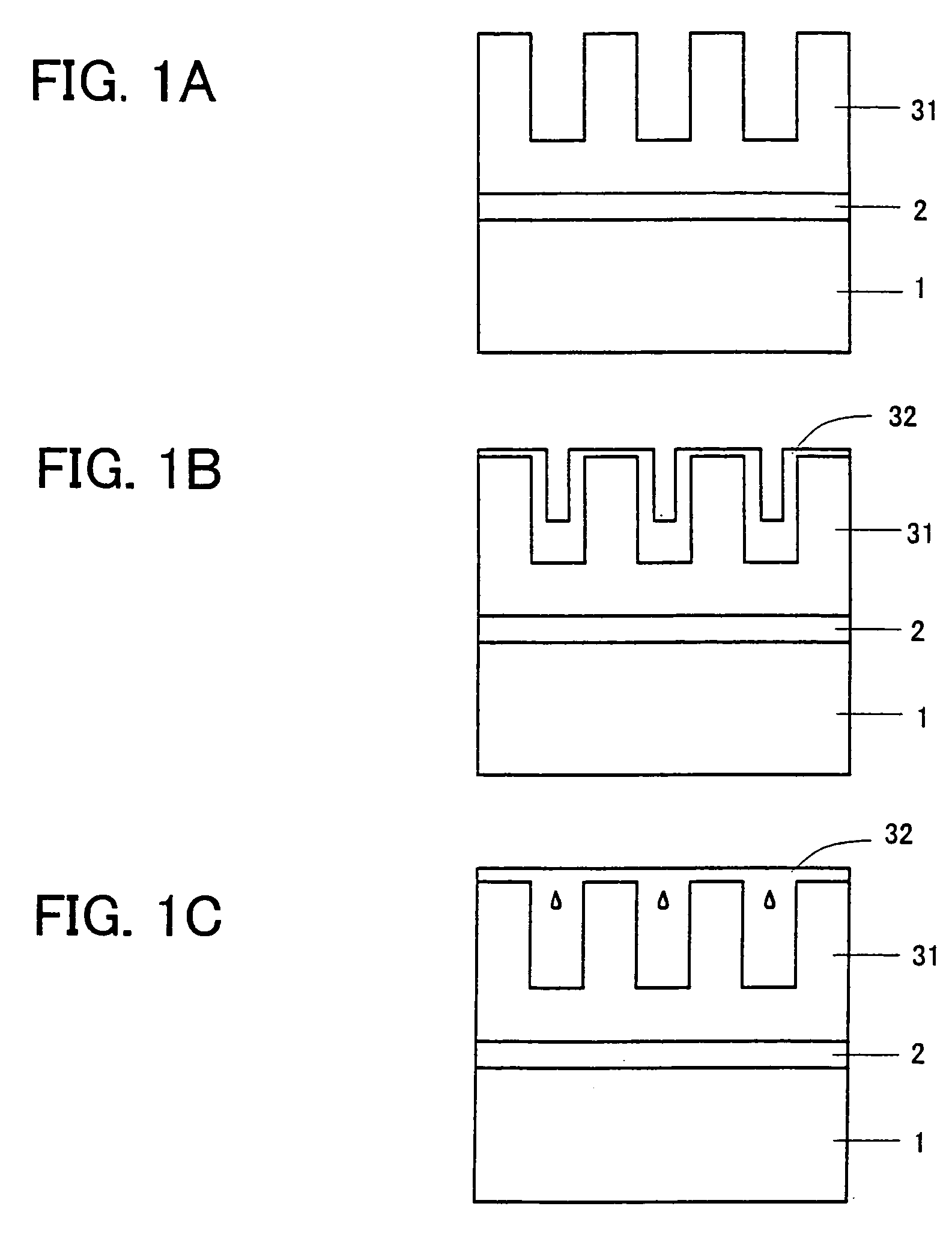
[0058]FIG. 1 shows the steps of the present embodiment. A monocrystalline sapphire substrate 1 was prepared such that the a-plane thereof cleaned through organic cleaning and heat treatment serves as the main surface thereof. Temperature was dropped to 400° C., and H2 (10 L / min), NH3 (5 L / min), and TMA (20 μmol / min) were supplied for approximately 3 minutes to thereby form, on the sapphire substrate 1, a buffer layer 2 of AlN having a thickness of approximately 40 nm. Next, while the temperature of the sapphire substrate 1 was maintained at 1000° C., H2 (20 L / min), NH3 (10 L / min), and TMG (300 μmol / min) were introduced to thereby form a GaN layer 31 having a thickness of approximately 3 μm.
[0059] By use of a hard bake resist mask, stripe-shaped trenches each having a width of 1 μm and a depth of 2 μm were selectively dry-etched at intervals of 1 μm by reactive ion beam etching (RIE). As a result, posts of the GaN layer 31 each having a width of 1 μm and tre...
second embodiment
[0061] [Second Embodiment]
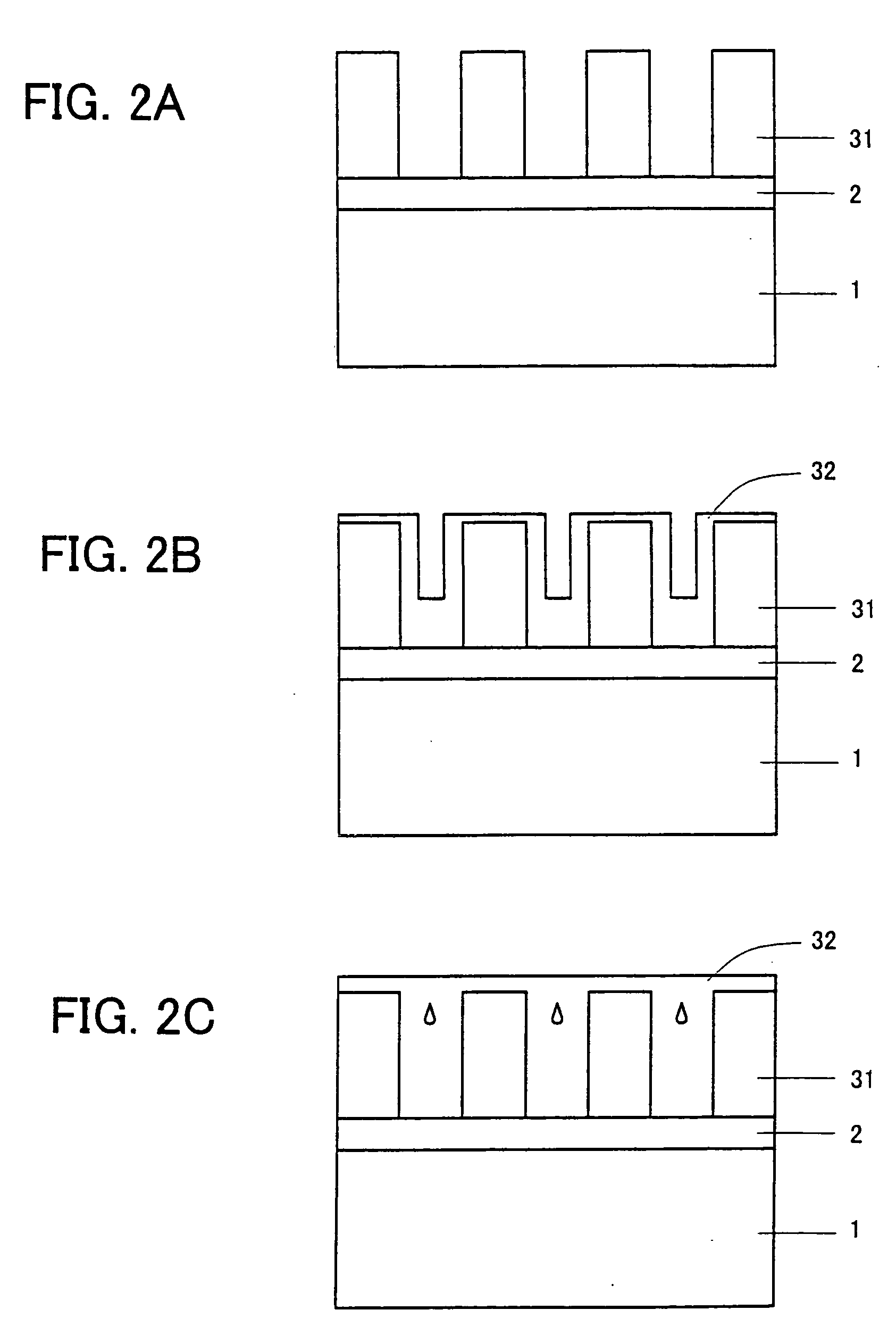
[0062] The present embodiment is illustrated in FIG. 2. A monocrystalline sapphire substrate 1 was prepared such that the a-plane thereof cleaned through organic cleaning and heat treatment serves as the main surface thereof. Temperature was dropped to 400° C., and H2 (10 L / min), NH3 (5 L / min), and TMA (20 μmol / min) were supplied for approximately 3 minutes to thereby form, on the sapphire substrate 1, an AlN layer 2 having a thickness of approximately 40 nm. Next, while the temperature of the sapphire substrate 1 was maintained at 1000° C., H2 (20 L / min), NH3 (10 L / min), and TMG (300 μmol / min) were introduced to thereby form a GaN layer 31 having a thickness of approximately 2 μm.
[0063] Next, by use of a hard bake resist mask, stripe-shaped trenches each having a width of 1 μm and a depth of 2 μm were selectively dry-etched at intervals of 1 μm by reactive ion beam etching (RIE). As a result, posts of the GaN layer 31 each having a width of 1 μm and a dep...
third embodiment
[0065] [Third Embodiment]
[0066] The present embodiment used an underlying layer comprising a plurality of layers as shown in FIG. 3. A monocrystalline sapphire substrate 1 was prepared such that the a-plane thereof cleaned through organic cleaning and heat treatment serves as the main surface thereof. Temperature was dropped to 400° C., and H2 (10 L / min), NH3 (5 L / min), and TMA (20 μmol / min) were supplied for approximately 3 minutes to thereby form, on the sapphire substrate 1, a first AlN layer (first buffer layer) 21 having a thickness of approximately 40 nm. Next, while the temperature of the sapphire substrate 1 was maintained at 1000° C., H2 (20 L / min), NH3 (10 L / min), and TMG (300 μmol / min) were introduced to thereby form a GaN layer (intermediate layer) 22 having a thickness of approximately 0.3 μm. Next, the temperature was dropped to 400° C., and H2 (10 L / min), NH3 (5 L / min), and TMA (20 μmol / min) were supplied for approximately 3 minutes to thereby form a second AlN layer ...
PUM
| Property | Measurement | Unit |
|---|---|---|
| thickness | aaaaa | aaaaa |
| thickness | aaaaa | aaaaa |
| thickness | aaaaa | aaaaa |
Abstract
Description
Claims
Application Information