Process for protecting solder joints and structure for alleviating electromigration and joule heating in solder joints

a solder joint and structure technology, applied in the direction of electrical apparatus, semiconductor devices, semiconductor/solid-state device details, etc., can solve the problems of serious reliability problems, heat dissipation, and electromigration in these small solder bumps, and achieve the effect of alleviating current crowding effect, and reducing the size of solder bumps

Inactive Publication Date: 2006-02-09
NAT CHIAO TUNG UNIV
View PDF4 Cites 29 Cited by
  • Summary
  • Abstract
  • Description
  • Claims
  • Application Information

AI Technical Summary

Benefits of technology

[0011] In order to relieve electromigration damage, the present process protects flip-chip solder joints, joints of anisotropic conductive film (ACF), and joints of tap automatic bond (TAB) by adding a thin layer of high electric resistivity materials in UBM of the c

Problems solved by technology

The size of these solder bumps is quite small because a large number of them is needed as chip-to-package interconnects.
Serious reliability problems arise with respect to thermal-mechanical fatigue, heat dissipation, and electromigration in these small solder bumps.
Since solder is a low melting point alloy having a fast atomic diffusion at ambient temperature, electromigration is a serious reliability concern.
Therefore, electromigration (EM) of the solder bumps has become an important issue.
In addition, when additional current (I) passes the metal (with resistance R), the metal is heated to higher temperature, i.e., Joule heating effect, so that the diffusion coefficient becomes larger, resulting in more serious electromigration; therefore, electromigration is a phenomenon that atoms transport due to the combination the electric and heating effects.
Moreover, in terms of flip-chip joints, the current crowding effect is generated at the joints of the solder and the conducting line due to their specific geometric shape (shown in FIG. 2), so that reliability problem arises since the above effect damage the joints of solders and the con

Method used


Image

  • Process for protecting solder joints and structure for alleviating electromigration and joule heating in solder joints
  • Process for protecting solder joints and structure for alleviating electromigration and joule heating in solder joints
  • Process for protecting solder joints and structure for alleviating electromigration and joule heating in solder joints

Examples


embodiment

[0038] The present embodiments include electromigration studies made through the following limited elemental analysis, IR temperature detection analysis, and actual solder bumps, however, the concepts and claims of the present invention are not limited thereto.

1. General Solder Production and Reliability

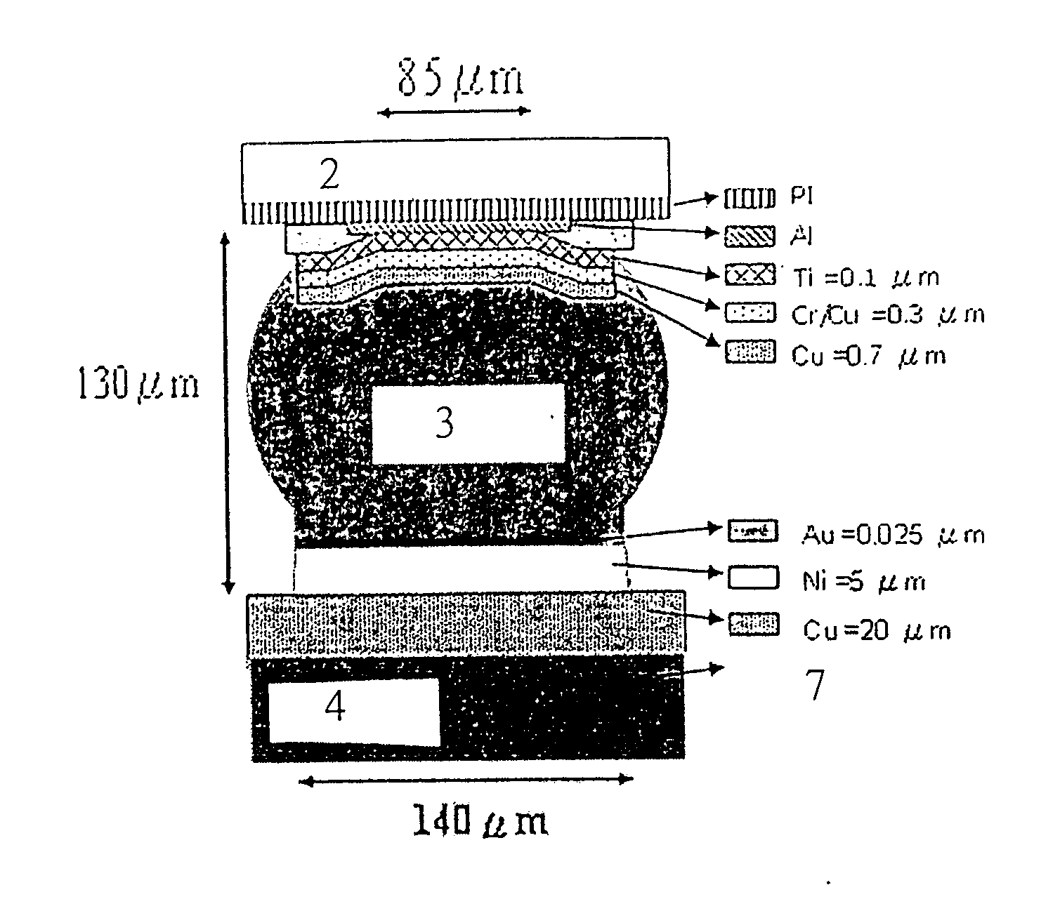
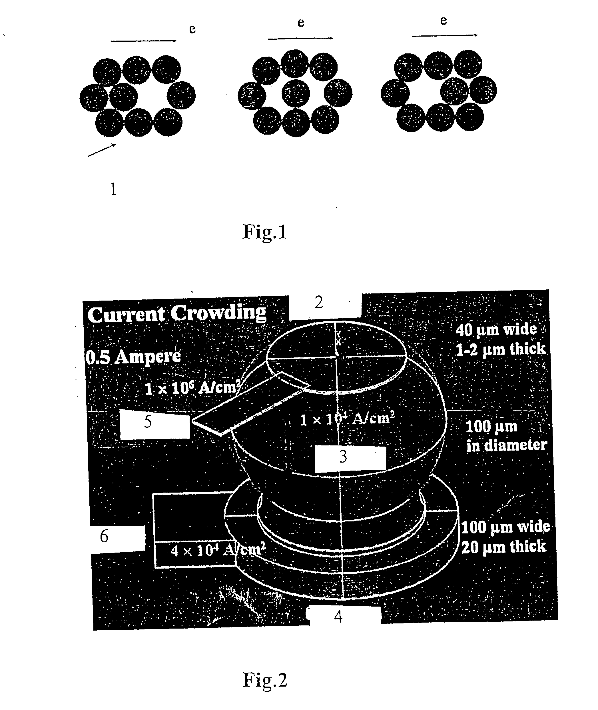
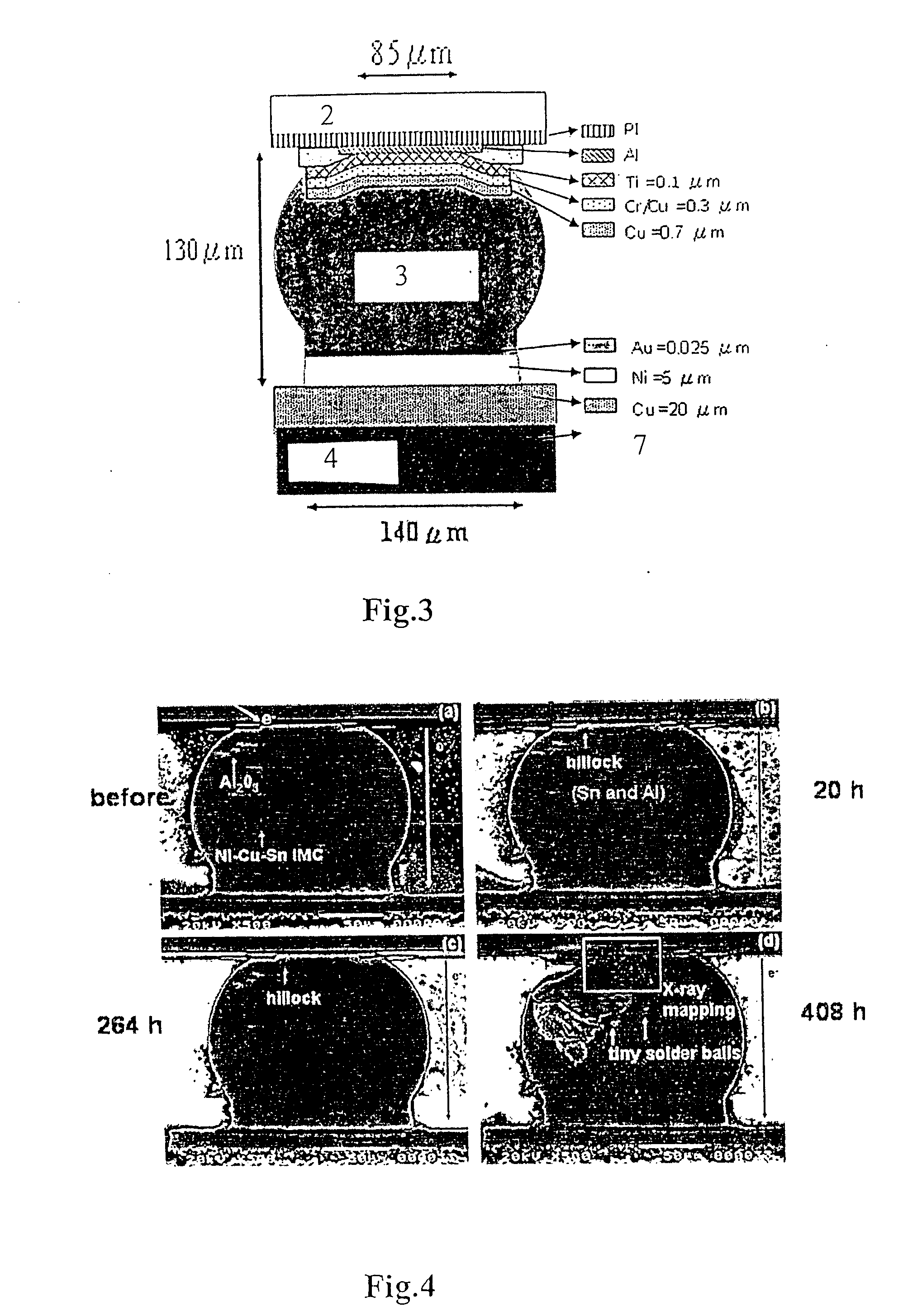
[0039] A current of 0.5 A was applied to solder bump 3 with the specific geometric shape shown in FIG. 2, the current density of aluminum lead and bump were 1×10⁷ and 1×10⁴ A / cm2 respectively, further, the resistance was 180 mΩ for aluminum lead 5 and 8 mΩ for bump 3. The resistance differences and the specific geometric shape enabled the majority of electrons moving toward the left side of the bump 3 then flowing down, and accelerated the damage of the joints between aluminum lead 5 and solder bump 3. In addition, Joule heating effect was larger in aluminum lead 5, thus temperature gradient was created in solder bump 3 to further promote the occurrence of electromigration, and cr...


PUM


Abstract

This invention provides a process for protecting solder joints, comprising forming an UBM or pad metallurgy in solder joints and then further forming a small solder bump on UBM or pad metallurgy between substrate and chip. Wherein a material of high electric resistance is coated at the ends of UBM or pad metallurgy where substrate is connected to chip, as to equalize the current distribution of solder bump, therefore the electromigration resistance of solder joints is improved by suppressing the current crowding and joule heating phenomenon.

Description

FIELD OF THE INVENTION [0001] The present invention provides a designing process for protecting joints including flip-chip solder joints, anisotropic conductive film (ACF) or tape automatic bond (TAB) joints, etc., in electronic packaging industry. The present invention alleviates current crowding effect of the solder bump and the electromigration damage, to prolong the life-time of the above joints. Current crowding results in local high current density region and causes local joule heating in solder joints. By suppressing the current crowding and joule heating phenomenon, the electromigration resistance of solder joints is improved and consequently the reliability of solder joints is enhanced. By suppressing current crowding, current flow paths are redistributed and become more uniform through a solder joint. Therefore, the current carrying capacity of each solder ball is increased and its effective resistance could be reduced under proper design. [0002] The present invention is w...

Claims


Application Information

Patent Timeline
IPC IPC(8): H01L23/48
CPCH01L24/10H01L2224/13099H01L24/13H01L2924/10253H01L2924/014H01L2924/01013H01L2924/01022H01L2924/01029H01L2924/01042H01L2924/01049H01L2924/01073H01L2924/01077H01L2924/01078H01L2924/01079H01L2924/01082H01L2924/01322H01L2924/04941H01L2924/04953H01L2924/14H01L2924/01006H01L2924/01023H01L2924/01024H01L2924/01033H01L2924/00H01L2224/13H01L2224/05022H01L2224/05001H01L2224/05124H01L2224/05147H01L2224/05166H01L2224/05171H01L2224/05647H01L2224/0518H01L2224/0568H01L2224/05686H01L24/05H01L24/81H01L24/16H01L24/03H01L2224/0401H01L2224/131H01L2924/00014H01L2924/013H01L2924/05442H01L2924/05042H01L2924/05432
Inventor CHEN, CHIHYEH, EVERETT CHANG-CHINGTU, KING-NING
Owner NAT CHIAO TUNG UNIV
Why Eureka
Try Eureka